MCB2470 Keil, MCB2470 Datasheet - Page 25
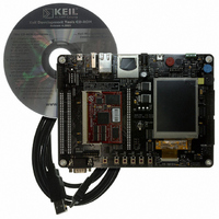
MCB2470
Manufacturer Part Number
MCB2470
Description
BOARD EVAL NXP LPC247X SERIES
Manufacturer
Keil
Type
MCUr
Specifications of MCB2470
Contents
Board, Cable, CD
For Use With/related Products
LPC2478
Lead Free Status / RoHS Status
Lead free / RoHS Compliant


NXP Semiconductors
Table 4.
[1]
[2]
[3]
[4]
[5]
[6]
[7]
[8]
LPC2478_1
Preliminary data sheet
Symbol
RESET
XTAL1
XTAL2
RTCX1
RTCX2
V
V
V
V
NC
V
V
VREF
VBAT
SSIO
SSCORE
SSA
DD(3V3)
DD(DCDC)(3V3)
DDA
5 V tolerant pad providing digital I/O functions with TTL levels and hysteresis.
5 V tolerant pad providing digital I/O functions (with TTL levels and hysteresis) and analog input. When configured as a ADC input,
digital section of the pad is disabled.
5 V tolerant pad providing digital I/O with TTL levels and hysteresis and analog output function. When configured as the DAC output,
digital section of the pad is disabled.
Open-drain 5 V tolerant digital I/O I
functionality. When power is switched off, this pin connected to the I
Pad provides digital I/O and USB functions. It is designed in accordance with the USB specification, revision 2.0 (Full-speed and
Low-speed mode only).
5 V tolerant pad with 5 ns glitch filter providing digital I/O functions with TTL levels and hysteresis.
5 V tolerant pad with 20 ns glitch filter providing digital I/O function with TTL levels and hysteresis.
Pad provides special analog functionality.
Pin description
Pin
35
44
46
34
36
33, 63,
77, 93,
114,133,
148,169,
189,
200
32, 84,
172
22
15, 60,
71, 89,
112,125,
146,
165,181,
198
30, 117,
141
26, 86,
174
20
24
38
[7]
[8]
[8]
[8]
[8]
[10]
[14]
[14]
[14]
[9]
[9]
[11]
[12]
[13]
…continued
Ball
M2
M4
N4
K2
L2
L3, T5,
R9,P12,
N16,
H14,
E15,
A12, B6,
A2
K4, P10,
D12
J2
G3,P6,
P8,U13,
P17,
K16,
C17,
B13,C9,
D7
G14
H4, P11,
D11
G4
K1
M3
J4, L14,
[8]
[10]
[8]
[9]
[14]
[8]
[11]
[14]
[7]
[8]
[14]
2
[13]
C-bus 400 kHz specification compatible pad. It requires an external pull-up to provide output
[9]
[12]
Type
I
I
O
I
O
I
I
I
I
I
I
I
I
I
Rev. 01 — 9 February 2007
Description
external reset input: A LOW on this pin resets the device, causing I/O
ports and peripherals to take on their default states, and processor
execution to begin at address 0. TTL with hysteresis, 5 V tolerant.
Input to the oscillator circuit and internal clock generator circuits.
Output from the oscillator amplifier.
Input to the RTC oscillator circuit.
Output from the RTC oscillator circuit.
ground: 0 V reference for the digital IO pins.
ground: 0 V reference for the core.
analog ground: 0 V reference. This should nominally be the same
voltage as V
3.3 V supply voltage: This is the power supply voltage for the I/O ports.
Not Connected pins: These pins must be left unconnected (floating).
3.3 V DC-to-DC converter supply voltage: This is the power supply for
the on-chip DC-to-DC converter.
analog 3.3 V pad supply voltage: This should be nominally the same
voltage as V
This voltage is used to power the ADC and DAC.
ADC reference: This should be nominally the same voltage as V
but should be isolated to minimize noise and error. The level on this pin is
used as a reference for ADC and DAC.
RTC power supply: 3.3 V on this pin supplies the power to the RTC.
SS
DD(3V3)
2
, but should be isolated to minimize noise and error.
C-bus is floating and does not disturb the I
but should be isolated to minimize noise and error.
Fast communication chip
2
LPC2478
C lines.
© NXP B.V. 2007. All rights reserved.
DD(3V3)
25 of 76
Related parts for MCB2470
Image
Part Number
Description
Manufacturer
Datasheet
Request
R

Part Number:
Description:
KIT REF SYSTEM 78K0 UPD78F0712
Manufacturer:
Renesas Electronics America
Datasheet:
Part Number:
Description:
KIT DEMO EVAL 78K0R IE3
Manufacturer:
Renesas Electronics America
Datasheet:
Part Number:
Description:
KIT EVAL SYSTEM 78K0 UPD78F0714
Manufacturer:
Renesas Electronics America
Datasheet:

Part Number:
Description:
KEIL C-COMPILER INTERNATIONAL
Manufacturer:
Silicon Laboratories Inc
Part Number:
Description:
KEIL C-COMPILER US VERSION
Manufacturer:
Silicon Laboratories Inc

Part Number:
Description:
DEV KIT FOR STM32
Manufacturer:
STMicroelectronics
Datasheet:

Part Number:
Description:
KIT STARTER FOR STM32
Manufacturer:
STMicroelectronics
Datasheet:

Part Number:
Description:
KIT STARTER FOR STM32F10XE MCU
Manufacturer:
STMicroelectronics
Datasheet:

Part Number:
Description:
KIT STARTER KEIL FOR STR910
Manufacturer:
STMicroelectronics
Datasheet:


Part Number:
Description:
Microcontroller Modules & Accessories KEIL ULINK PRO 5V ADAPTOR KIT
Manufacturer:
Keil Software

Part Number:
Description:
BOARD EVAL FOR LPC213X ARM MCU
Manufacturer:
NXP Semiconductors
Datasheet:

Part Number:
Description:
K60N512 Keil Tower Kit
Manufacturer:
Freescale Semiconductor
Datasheet: