MCB2470 Keil, MCB2470 Datasheet - Page 24
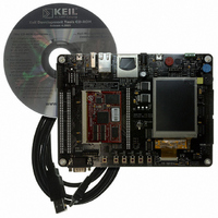
MCB2470
Manufacturer Part Number
MCB2470
Description
BOARD EVAL NXP LPC247X SERIES
Manufacturer
Keil
Type
MCUr
Specifications of MCB2470
Contents
Board, Cable, CD
For Use With/related Products
LPC2478
Lead Free Status / RoHS Status
Lead free / RoHS Compliant


NXP Semiconductors
Table 4.
LPC2478_1
Preliminary data sheet
Symbol
P4[23]/A23/
RXD2/MOSI1
P4[24]/OE
P4[25]/WE
P4[26]/BLS0
P4[27]/BLS1
P4[28]/BLS2/
MAT2[0]/LCD[6]/
LCD[10]/LCD[2]/
TXD3
P4[29]/BLS3/
MAT2[1]
LCD[7]/LCD[11]/
LCD[3]/RXD3
P4[30]/CS0
P4[31]/CS1
ALARM
USB_D−2
DBGEN
TDO
TDI
TMS
TRST
TCK
RTCK
RSTOUT
Pin description
Pin
129
183
179
119
139
170
176
187
193
37
52
9
2
4
6
8
10
206
29
[1]
[1]
[1]
[1]
[1]
[8]
[1]
[1]
[1]
[1]
[1]
[1]
[1]
[1]
[1]
[1]
[1]
[1]
…continued
Ball
J15
B8
B9
L15
G15
C11
B10
B7
A4
N1
U1
F4
D3
C2
E3
D1
E2
C3
K3
[1]
[1]
[1]
[1]
[1]
[1]
[1]
[1]
[8]
[1]
[1]
[1]
[1]
[1]
[1]
[1]
[1]
[1]
Type
I/O
I/O
I
I/O
I/O
O
I/O
O
I/O
O
I/O
O
I/O
O
O
O
O
I/O
O
O
O
I
I/O
O
I/O
O
O
I/O
I
O
I
I
I
I
I/O
O
Rev. 01 — 9 February 2007
Description
P4[23] — General purpose digital input/output pin.
A23 — External memory address line 23.
RXD2 — Receiver input for UART2.
MOSI1 — Master Out Slave In for SSP1.
P4[24] — General purpose digital input/output pin.
OE — LOW active Output Enable signal.
P4[25] — General purpose digital input/output pin.
WE — LOW active Write Enable signal.
P4[26] — General purpose digital input/output pin.
BLS0 — LOW active Byte Lane select signal 0.
P4[27] — General purpose digital input/output pin.
BLS1 — LOW active Byte Lane select signal 1.
P4 [28] — General purpose digital input/output pin.
BLS2 — LOW active Byte Lane select signal 2.
MAT2[0] — Match output for Timer 2, channel 0.
LCD[6]/LCD[10]/LCD[2] — LCD data.
TXD3 — Transmitter output for UART3.
P4[29] — General purpose digital input/output pin.
BLS3 — LOW active Byte Lane select signal 3.
MAT2[1] — Match output for Timer 2, channel 1.
LCD[7]/LCD[11]/LCD[3] — LCD data.
RXD3 — Receiver input for UART3.
P4[30] — General purpose digital input/output pin.
CS0 — LOW active Chip Select 0 signal.
P4[31] — General purpose digital input/output pin.
CS1 — LOW active Chip Select 1 signal.
ALARM — RTC controlled output. This is a 1.8 V pin. It goes HIGH when
a RTC alarm is generated.
USB_D−2 — USB port 2 bidirectional D− line.
DBGEN — JTAG interface control signal. Also used for boundary
scanning.
TDO — Test Data out for JTAG interface.
TDI — Test Data in for JTAG interface.
TMS — Test Mode Select for JTAG interface.
TRST — Test Reset for JTAG interface.
TCK — Test Clock for JTAG interface.
RTCK — JTAG interface control signal.
Note: LOW on this pin while RESET is LOW enables ETM pins (P2[9:0])
to operate as Trace port after reset.
RSTOUT — This is a 1.8 V pin. LOW on this pin indicates LPC2478
being in Reset state.
[19]
[19]
Fast communication chip
[19]
[19]
LPC2478
© NXP B.V. 2007. All rights reserved.
24 of 76
Related parts for MCB2470
Image
Part Number
Description
Manufacturer
Datasheet
Request
R

Part Number:
Description:
KIT REF SYSTEM 78K0 UPD78F0712
Manufacturer:
Renesas Electronics America
Datasheet:
Part Number:
Description:
KIT DEMO EVAL 78K0R IE3
Manufacturer:
Renesas Electronics America
Datasheet:
Part Number:
Description:
KIT EVAL SYSTEM 78K0 UPD78F0714
Manufacturer:
Renesas Electronics America
Datasheet:

Part Number:
Description:
KEIL C-COMPILER INTERNATIONAL
Manufacturer:
Silicon Laboratories Inc
Part Number:
Description:
KEIL C-COMPILER US VERSION
Manufacturer:
Silicon Laboratories Inc

Part Number:
Description:
DEV KIT FOR STM32
Manufacturer:
STMicroelectronics
Datasheet:

Part Number:
Description:
KIT STARTER FOR STM32
Manufacturer:
STMicroelectronics
Datasheet:

Part Number:
Description:
KIT STARTER FOR STM32F10XE MCU
Manufacturer:
STMicroelectronics
Datasheet:

Part Number:
Description:
KIT STARTER KEIL FOR STR910
Manufacturer:
STMicroelectronics
Datasheet:


Part Number:
Description:
Microcontroller Modules & Accessories KEIL ULINK PRO 5V ADAPTOR KIT
Manufacturer:
Keil Software

Part Number:
Description:
BOARD EVAL FOR LPC213X ARM MCU
Manufacturer:
NXP Semiconductors
Datasheet:

Part Number:
Description:
K60N512 Keil Tower Kit
Manufacturer:
Freescale Semiconductor
Datasheet: