MCB2470 Keil, MCB2470 Datasheet - Page 11
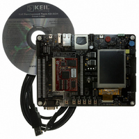
MCB2470
Manufacturer Part Number
MCB2470
Description
BOARD EVAL NXP LPC247X SERIES
Manufacturer
Keil
Type
MCUr
Specifications of MCB2470
Contents
Board, Cable, CD
For Use With/related Products
LPC2478
Lead Free Status / RoHS Status
Lead free / RoHS Compliant


NXP Semiconductors
Table 4.
LPC2478_1
Preliminary data sheet
Symbol
P0[7]/I2STX_CLK/
LCD[9]/SCK1/
MAT2[1]
P0[8]/I2STX_WS/
LCD[16]/
MISO1/MAT2[2]
P0[9]/I2STX_SDA/
LCD[17]/
MOSI1/MAT2[3]
P0[10]/TXD2/
SDA2/MAT3[0]
P0[11]/RXD2/
SCL2/MAT3[1]
P0[12]/
USB_PPWR2/
MISO1/AD0[6]
P0[13]/
USB_UP_LED2/
MOSI1/AD0[7]
Pin description
Pin
162
160
158
98
100
41
45
[1]
[2]
[2]
[1]
[1]
[1]
[1]
…continued
Ball
C13
A15
C14
T15
R14
R1
R2
[2]
[2]
[1]
[1]
[1]
[1]
[1]
Type
I/O
I/O
O
I/O
O
I/O
I/O
O
I/O
O
I/O
I/O
O
I/O
O
I/O
O
I/O
O
I/O
I
I/O
O
I/O
O
I/O
I
I/O
O
I/O
I
Rev. 01 — 9 February 2007
Description
P0[7] — General purpose digital input/output pin.
I2STX_CLK — I
by the slave. Corresponds to the signal SCK in the I
specification.
LCD[9] — LCD data.
SCK1 — Serial Clock for SSP1.
MAT2[1] — Match output for Timer 2, channel 1.
P0[8] — General purpose digital input/output pin.
I2STX_WS — I
received by the slave. Corresponds to the signal WS in the I
specification.
LCD[16] — LCD data.
MISO1 — Master In Slave Out for SSP1.
MAT2[2] — Match output for Timer 2, channel 2.
P0[9] — General purpose digital input/output pin.
I2STX_SDA — I
by the receiver. Corresponds to the signal SD in the I
specification.
LCD[17] — LCD data.
MOSI1 — Master Out Slave In for SSP1.
MAT2[3] — Match output for Timer 2, channel 3.
P0[10] — General purpose digital input/output pin.
TXD2 — Transmitter output for UART2.
SDA2 — I
MAT3[0] — Match output for Timer 3, channel 0.
P0[11] — General purpose digital input/output pin.
RXD2 — Receiver input for UART2.
SCL2 — I
MAT3[1] — Match output for Timer 3, channel 1.
P0[12] — General purpose digital input/output pin.
USB_PPWR2 — Port Power enable signal for USB port 2.
MISO1 — Master In Slave Out for SSP1.
AD0[6] — A/D converter 0, input 6.
P0[13] — General purpose digital input/output pin.
USB_UP_LED2 — USB port 2 GoodLink LED indicator. It is LOW when
device is configured (non-control endpoints enabled). It is HIGH when the
device is not configured or during global suspend.
MOSI1 — Master Out Slave In for SSP1.
AD0[7] — A/D converter 0, input 7.
2
2
C2 clock input/output (this is not an open-drain pin).
C2 data input/output (this is not an open-drain pin).
[15]
[15]
[15]
2
2
S Transmit word select. It is driven by the master and
2
S transmit clock. It is driven by the master and received
S transmit data. It is driven by the transmitter and read
[15]
[15]
[15]
Fast communication chip
2
LPC2478
S-bus
2
© NXP B.V. 2007. All rights reserved.
S-bus
2
S-bus
11 of 76
Related parts for MCB2470
Image
Part Number
Description
Manufacturer
Datasheet
Request
R

Part Number:
Description:
KIT REF SYSTEM 78K0 UPD78F0712
Manufacturer:
Renesas Electronics America
Datasheet:
Part Number:
Description:
KIT DEMO EVAL 78K0R IE3
Manufacturer:
Renesas Electronics America
Datasheet:
Part Number:
Description:
KIT EVAL SYSTEM 78K0 UPD78F0714
Manufacturer:
Renesas Electronics America
Datasheet:

Part Number:
Description:
KEIL C-COMPILER INTERNATIONAL
Manufacturer:
Silicon Laboratories Inc
Part Number:
Description:
KEIL C-COMPILER US VERSION
Manufacturer:
Silicon Laboratories Inc

Part Number:
Description:
DEV KIT FOR STM32
Manufacturer:
STMicroelectronics
Datasheet:

Part Number:
Description:
KIT STARTER FOR STM32
Manufacturer:
STMicroelectronics
Datasheet:

Part Number:
Description:
KIT STARTER FOR STM32F10XE MCU
Manufacturer:
STMicroelectronics
Datasheet:

Part Number:
Description:
KIT STARTER KEIL FOR STR910
Manufacturer:
STMicroelectronics
Datasheet:


Part Number:
Description:
Microcontroller Modules & Accessories KEIL ULINK PRO 5V ADAPTOR KIT
Manufacturer:
Keil Software

Part Number:
Description:
BOARD EVAL FOR LPC213X ARM MCU
Manufacturer:
NXP Semiconductors
Datasheet:

Part Number:
Description:
K60N512 Keil Tower Kit
Manufacturer:
Freescale Semiconductor
Datasheet: