XE8000EV110 Semtech, XE8000EV110 Datasheet - Page 122
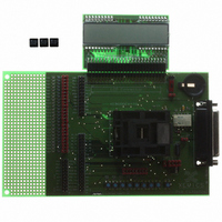
XE8000EV110
Manufacturer Part Number
XE8000EV110
Description
EVAL BOARD FOR XE8802AMI035LF
Manufacturer
Semtech
Type
MCUr
Specifications of XE8000EV110
Contents
Fully Assembled Evaluation Board
For Use With/related Products
XE88LC02MI035
Lead Free Status / RoHS Status
Contains lead / RoHS non-compliant


17.6.1
Depending on the application objectives, the user may enable or bypass each PGA stage. This is done using the
word ENABLE and the coding given in Table 17-13. To reduce power dissipation, the ADC can also be inactivated
while idle.
17.6.2
The first stage can have a buffer function (unity gain) or provide a gain of 10 (see Table 17-14). The voltage V
the output of PGA1 is:
where GD
17.6.3
The second PGA has a finer gain and offset tuning capability, as shown in Table 17-15 and Table 17-16. The
voltage V
where GD
PGA2_GAIN[1:0] and PGA2_OFFSET[3:0] .
17.6.4
The finest gain and offset tuning is performed with the third and last PGA stage, according to the coding of Table
17-17 and Table 17-18. The output of PGA3 is also the input of the ADC. Thus, similarly to PGA2, we find that the
voltage entering the ADC is given by:
© Semtech 2006
V
V
D2
D
D
1
2
1
2
PGA & ADC Enabling
PGA1
PGA2
PGA3
is the gain of PGA1 (in V/V) controlled with the bit PGA1_GAIN.
at the output of PGA2 is given by:
and GDoff
=
=
GD
GD
1
2
⋅
⋅
V
V
IN
D
1
2
−
are respectively the gain and offset of PGA2 (in V/V). These are controlled with the words
GDoff
2
(V)
⋅
V
REF
PGA3_OFFSET[6:0]
(V)
0000000
0000001
0000010
0010000
0100000
0111111
1000000
1000001
1000010
1010000
1100000
1111111
Table 17-18. PGA3 offset settings
XE8802 Sensing Machine Data Acquisition MCU
...
...
...
...
...
...
17-10
with ZoomingADC™ and LCD driver
+1/12(=+0.083)
+63/12(=+5.25)
-1/12(=-0.083)
-63/12(=-5.25)
PGA3 Offset
GDoff
+16/12
+32/12
-16/12
-32/12
+2/12
-2/12
...
...
...
...
...
...
0
0
3
(V/V)
(Eq. 5)
(Eq. 6)
www.semtech.com
D1
at
Related parts for XE8000EV110
Image
Part Number
Description
Manufacturer
Datasheet
Request
R

Part Number:
Description:
EVALUATION BOARD
Manufacturer:
Semtech
Datasheet:
Part Number:
Description:
EVALUATION BOARD
Manufacturer:
Semtech
Datasheet:
Part Number:
Description:
VOLTAGE SUPPRESSOR, TRANSIENT SEMTECH
Manufacturer:
Semtech
Datasheet:

Part Number:
Description:
HIGH VOLTAGE CAPACITORS MONOLITHIC CERAMIC TYPE
Manufacturer:
Semtech Corporation
Datasheet:
Part Number:
Description:
EZ1084CM5.0 AMP POSITIVE VOLTAGE REGULATOR
Manufacturer:
Semtech Corporation
Datasheet:
Part Number:
Description:
3.0 AMP LOW DROPOUT POSITIVE VOLTAGE REGULATORS
Manufacturer:
Semtech Corporation
Datasheet:
Part Number:
Description:
Manufacturer:
Semtech Corporation
Datasheet:
Part Number:
Description:
RailClamp Low Capacitance TVS Diode Array
Manufacturer:
Semtech Corporation
Datasheet:
Part Number:
Description:
Manufacturer:
Semtech Corporation
Datasheet:
Part Number:
Description:
Manufacturer:
Semtech Corporation
Datasheet:
Part Number:
Description:
Manufacturer:
Semtech Corporation
Datasheet:
Part Number:
Description:
Manufacturer:
Semtech Corporation
Datasheet: