QSK-62P PLUS BNS Solutions, QSK-62P PLUS Datasheet - Page 86
QSK-62P PLUS
Manufacturer Part Number
QSK-62P PLUS
Description
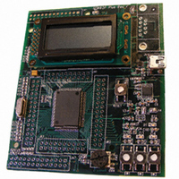
KIT QUICK START RENESAS 62P
Manufacturer
BNS Solutions
Series
M16C™r
Type
MCUr
Datasheet
1.QSK-62P_PLUS.pdf
(103 pages)
Specifications of QSK-62P PLUS
Contents
Board, Cable, CD
For Use With/related Products
M16C/62P
Lead Free Status / RoHS Status
Not applicable / Not applicable
Other names
867-1000
QSK-62P
QSK26A
QSK62P
QSK-62P
QSK26A
QSK62P


M16C/62P Group (M16C/62P, M16C/62PT)
Rev.2.41
REJ03B0001-0241
Table 5.51
NOTES:
Table 5.52
NOTES:
−
INL
−
−
DNL
−
−
R
t
t
t
V
V
−
−
t
R
I
CONV
CONV
SAMP
SU
VREF
REF
IA
LADDER
O
Symbol
Symbol
1. Referenced to V
2. φ AD frequency must be 12 MHz or less.
3. When sample & hold is disabled, φ AD frequency must be 250 kHz or more, in addition to the limitation in Note 2.
1. Referenced to V
2. This applies when using one D/A converter, with the D/A register for the unused D/A converter set to “00h”. The resistor
T version = − 40 to 85 ° C, V version = − 40 to 125 ° C
When sample & hold is enabled, φ AD frequency must be 1MHz or more, in addition to the limitation in Note 2.
version = − 40 to 85 ° C, V version = − 40 to 125 ° C
ladder of the A/D converter is not included. Also, when D/A register contents are not “00h”, the I
disconnected by the A/D control register.
Jan 10, 2006
Resolution
Integral Non-Linearity
Error
Absolute Accuracy
Tolerance Level Impedance
Differential Non-Linearity Error
Offset Error
Gain Error
Ladder Resistance
10-bit Conversion Time, Sample & Hold
Function Available
8-bit Conversion Time, Sample & Hold
Function Available
Sampling Time
Reference Voltage
Analog Input Voltage
Resolution
Absolute Accuracy
Setup Time
Output Resistance
Reference Power Supply Input Current
A/D Conversion Characteristics
D/A Conversion Characteristics
CC1
CC1
=AV
=V
Page 84 of 96
REF
CC
Parameter
Parameter
=4.0 to 5.5V, V
=V
REF
=4.0 to 5.5V, V
10bit
8bit
10bit
8bit
SS
=AV
SS
SS
=AV
=0V at T
V
V
V
5V
V
V
V
5V
V
V
V
V
(1)
REF
REF
CC1
REF
REF
CC1
REF
REF
REF
REF
SS
(1)
=0V at T
(NOTE 2)
=V
=
=
=V
=
=
=V
=V
=V
=V
opr
Measuring Condition
CC1
CC1
CC1
CC1
CC1
CC1
Measuring Condition
AN0 to AN7 input,
AN0_0 to AN0_7 input,
AN2_0 to AN2_7 input,
ANEX0, ANEX1 input
External operation amp
connection mode
AN0 to AN7 input,
AN0_0 to AN0_7 input,
AN2_0 to AN2_7 input,
ANEX0, ANEX1 input
External operation amp
connection mode
= − 40 to 85 ° C / − 40 to 125 ° C unless otherwise specified. T
=5V
=5V
=5V, φ AD=12MHz
=5V, φ AD=12MHz
opr
= − 40 to 85 ° C / − 40 to 125 ° C unless otherwise specified.
Min.
Min.
2.75
2.33
0.25
4
2.0
10
0
5. Electrical Characteristics
VREF
Standard
Standard
Typ.
Typ.
10
will flow even if Vref id
3
Max.
Max.
V
V
1.0
1.5
20
10
40
±3
±7
±2
±3
±7
±2
±1
±3
±3
8
3
CC1
REF
Unit
Unit
LSB
LSB
LSB
LSB
LSB
LSB
LSB
LSB
LSB
Bits
Bits
mA
k Ω
k Ω
k Ω
µ s
µ s
µ s
µ s
%
V
V