QSK-62P PLUS BNS Solutions, QSK-62P PLUS Datasheet - Page 65
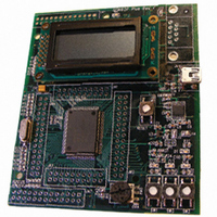
QSK-62P PLUS
Manufacturer Part Number
QSK-62P PLUS
Description
KIT QUICK START RENESAS 62P
Manufacturer
BNS Solutions
Series
M16C™r
Type
MCUr
Datasheet
1.QSK-62P_PLUS.pdf
(103 pages)
Specifications of QSK-62P PLUS
Contents
Board, Cable, CD
For Use With/related Products
M16C/62P
Lead Free Status / RoHS Status
Not applicable / Not applicable
Other names
867-1000
QSK-62P
QSK26A
QSK62P
QSK-62P
QSK26A
QSK62P


M16C/62P Group (M16C/62P, M16C/62PT)
Rev.2.41
REJ03B0001-0241
Figure 5.10
Memory Expansion Mode, Microprocessor Mode
(For 1- or 2-wait setting, external area access and multiplex bus selection )
Read timing
Write timing
BCLK
CSi
ADi
/DBi
ADi
BHE
ALE
RD
BCLK
CSi
ADi
/DBi
ADi
BHE
ALE
WR,WRL,
WRH
Measuring conditions
· V
· Input timing voltage : V
· Output timing voltage : V
CC1
Jan 10, 2006
=V
CC2
Timing Diagram (8)
=5V
t
d(BCLK-ALE)
t
d(BCLK-CS)
t
d(BCLK-ALE)
(0.5×t
25ns.max
t
t
t
25ns.max
t
25ns.max
t
d(BCLK-AD)
d(BCLK-CS)
25ns.max
d(BCLK-AD)
d(AD-ALE)
(0.5×t
25ns.max
25ns.max
d(AD-ALE)
Page 63 of 96
cyc
cyc
-25)ns.min
IL
-25)ns.min
Address
Address
=0.8V, V
OL
=0.4V, V
t
t
h(BCLK-ALE)
h(BCLK-ALE)
−4ns.min
−4ns.min
IH
=2.0V
OH
=2.4V
t
d(BCLK-RD)
t
t
d(BCLK-DB)
h(ALE-AD)
(0.5×t
t
40ns.max
25ns.max
25ns.max
d(BCLK-WR)
t
d(AD-WR)
0ns.min
t
t
0ns.min
cyc
dZ(RD-AD)
8ns.max
d(AD-RD)
t
-15)ns.min
cyc
t
cyc
(1.5×t
(1.5×t
Data output
t
t
d(DB-WR)
cyc
ac3(RD-DB)
cyc
-40)ns.min
-45)ns.max
t
Data input
su(DB-RD)
40ns.min
(0.5×t
(0.5×t
cyc
V
cyc
t
-10)ns.min
t
(0.5×t
h(RD-CS)
(0.5×t
t
h(BCLK-WR)
CC1
h(BCLK-RD)
-10)ns.min
(0.5×t
t
h(WR-CS)
t
0ns.min
0ns.min
t
t
5. Electrical Characteristics
h(RD-AD)
t
cyc
h(WR-AD)
h(RD-DB)
0ns.min
cyc
h(WR-DB)
cyc
-10)ns.min
-10)ns.min
-10)ns.min
=V
t
t
CC2
h(BCLK-AD)
h(BCLK-AD)
t
h(BCLK-CS)
t
4ns.min
4ns.min
h(BCLK-CS)
t
4ns.min
4ns.min
h(BCLK-DB)
4ns.min
Address
Address
=5V