ADIS16100/PCB Analog Devices Inc, ADIS16100/PCB Datasheet - Page 5
ADIS16100/PCB
Manufacturer Part Number
ADIS16100/PCB
Description
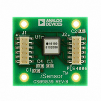
BOARD EVALUATION ADIS16100
Manufacturer
Analog Devices Inc
Series
iSensor™r
Specifications of ADIS16100/PCB
Sensor Type
Gyroscope, 1 Axis
Sensing Range
±300°/sec
Interface
SPI Serial
Voltage - Supply
4.75 V ~ 5.25 V
Embedded
No
Utilized Ic / Part
ADIS16100
Silicon Manufacturer
Analog Devices
Application Sub Type
Angular Rate Sensor / Gyroscope
Kit Application Type
Sensing - Motion / Vibration / Shock
Silicon Core Number
ADIS16100
Kit Contents
Board
Lead Free Status / RoHS Status
Contains lead / RoHS non-compliant
For Use With
ADISUSBZ - KIT EVAL ADIS W/SOFTWARE USBADISEVALZ - KIT PC EVALUATION W/SOFTWARE
Sensitivity
-
Lead Free Status / Rohs Status
Not Compliant


TIMING SPECIFICATIONS
T
Table 2.
Parameter
f
t
t
t
t
t
t
t
t
t
t
t
t
1
2
3
4
SCLK
CONVERT
QUIET
2
3
4
5
6
7
8
9
10
11
Guaranteed by design. All input signals are specified with t
from 4.75 V to 5.25 V.
Mark/space ratio for the SCLK input is 40/60 to 60/40.
Measured with the load circuit in Figure 3 and defined as the time required for the output to cross 0.4 V or 0.7 × V
t
back to remove the effects of charging or discharging the 50 pF capacitor. The time, t
and is independent of the bus loading.
A
3
3
4
8
is derived from the measured time taken by the data outputs to change 0.5 V when loaded with the circuit in Figure 3. The measured number is then extrapolated
= 25°C, angular rate = 0°/sec, unless otherwise noted.
2
DOUT
SCLK
THREE-STATE
DIN
CS
t
V
10
20
16 × t
50
10
30
40
0.4 × t
0.4 × t
10
15/35
10
5
20
t
2
3
CC
= V
ZERO
WRITE
SCLK
SCLK
SCLK
DRIVE
1
ZERO
= 5 V
t
LOW
9
2
ADD1
ADDRESS BITS
DONTC
Unit
kHz min
MHz max
ns min
ns min
ns max
ns max
ns min
ns min
ns min
ns min/max
ns min
ns min
ns min
3
t
ADD0
4
DONTC
Figure 3. Load Circuit for Digital Output Timing Specifications
Figure 2. Gyroscope Serial Interface Timing Diagram
4
R
D
and t
B11
TO OUTPUT
Description
Minimum quiet time required between CS rising edge and start of next conversion.
CS to SCLK setup time.
Delay from CS until DOUT three-state disabled.
Data access time after SCLK falling edge.
SCLK low pulse width.
SCLK high pulse width.
SCLK to DOUT valid hold time.
SCLK falling edge to DOUT high impedance.
DIN setup time prior to SCLK falling edge.
DIN hold time after SCLK falling edge.
16
t
ADD1
6
th
F
SCLK falling edge to CS high.
= 5 ns (10% to 90% of V
5
1
t
DB10
7
PIN
t
CONVERT
ADD0
t
50pF
10
Rev. D | Page 5 of 16
C
6
L
200µA
200µA
8
11
, quoted in the Timing Specifications is the true bus relinquish time of the part
DB4
CODING
CC
I
I
OL
OH
) and timed from a voltage level of 1.6 V. The 5 V operating range spans
12
DB3
DONT
1.6V
13
C
DB2
DONTC
B
DRIVE
14
t
5
.
DB1
DONTC
15
t
8
DB0
DONTC
16
THREE-STATE
t
11
t
QUIET
ADIS16100
Related parts for ADIS16100/PCB
Image
Part Number
Description
Manufacturer
Datasheet
Request
R

Part Number:
Description:
±1.7g Dual-Axis IMEMS Accelerometer Evaluation Board
Manufacturer:
Analog Devices Inc
Datasheet:

Part Number:
Description:
Inertial Sensor Evaluation System
Manufacturer:
Analog Devices Inc
Datasheet:
Part Number:
Description:
Manufacturer:
Analog Devices Inc
Datasheet:
Part Number:
Description:
Manufacturer:
Analog Devices Inc
Datasheet:
Part Number:
Description:
Manufacturer:
Analog Devices Inc
Datasheet:
Part Number:
Description:
Manufacturer:
Analog Devices Inc
Datasheet:
Part Number:
Description:
Manufacturer:
Analog Devices Inc
Datasheet:
Part Number:
Description:
Manufacturer:
Analog Devices Inc
Datasheet:
Part Number:
Description:
Manufacturer:
Analog Devices Inc
Datasheet:
Part Number:
Description:
Manufacturer:
Analog Devices Inc
Datasheet:
Part Number:
Description:
Manufacturer:
Analog Devices Inc
Datasheet:
Part Number:
Description:
Manufacturer:
Analog Devices Inc
Datasheet:
Part Number:
Description:
Manufacturer:
Analog Devices Inc
Datasheet: