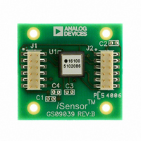
ADIS16100/PCB Analog Devices Inc, ADIS16100/PCB Datasheet

ADIS16100/PCB
Manufacturer Part Number
ADIS16100/PCB
Description
BOARD EVALUATION ADIS16100
Manufacturer
Analog Devices Inc
Series
iSensor™r
Specifications of ADIS16100/PCB
Sensor Type
Gyroscope, 1 Axis
Sensing Range
±300°/sec
Interface
SPI Serial
Voltage - Supply
4.75 V ~ 5.25 V
Embedded
No
Utilized Ic / Part
ADIS16100
Silicon Manufacturer
Analog Devices
Application Sub Type
Angular Rate Sensor / Gyroscope
Kit Application Type
Sensing - Motion / Vibration / Shock
Silicon Core Number
ADIS16100
Kit Contents
Board
Lead Free Status / RoHS Status
Contains lead / RoHS non-compliant
For Use With
ADISUSBZ - KIT EVAL ADIS W/SOFTWARE USBADISEVALZ - KIT PC EVALUATION W/SOFTWARE
Sensitivity
-
Lead Free Status / Rohs Status
Not Compliant
Preliminary Technical Data
GENERAL DESCRIPTION
The ADIS16100/PCB is a simple evaluation board that provides
convenient access to the ADIS16100 using a standard 2mm,
2x6, connector interface. These connectors can be accessed
using a variety of cable options, including standard 1mm ribbon
cables. The ADIS16100/PCB is designed to be evaluated in an
existing digital platform (MCU, DSP, FPGA, PLD, etc) or as
part of the ADISEVAL system. Four mounting holes (sized for
2-56 or 2mm screws) have been provided to secure the board
during evaluation.
CIRCUIT DESCRIPTION
The schematic, layout and parts list for the ADIS16100/PCB can
be found in Figure 1, Figure 2, and Table 1.
The ADIS16100’s digitized outputs can be accessed using the 4-
wire serial port interface (SPI) signals on J1: SCLK, CS, DOUT
and DIN. For specific information on using the ADIS16100’s
SPI interface, refer to the ADIS16100 datasheet. Auxiliary
functions, such as the two 12-bit ADC inputs, can be accessed
using J2. C1 and C4 provide additional filtering for the two
different power supply inputs (Vdrive and Vcc). The
ADIS16100’s reference voltage is filtered by C2.
Reference Designator
U1
J1,J2
C1, C4
C2
C3
SPECIAL NOTES ON HANDLING
Note that the ADIS16100/PCB is not reverse polarity protected.
Reversing the power supply or applying inappropriate voltages
to any pin (outside the Absolute Maximum Ratings in the
ADIS16100 data sheet) may damage the ADIS16100/PCB.
Vcc
Vdrive
Rev. PrD
Information furnished by Analog Devices is believed to be accurate and reliable.
However, no responsibility is assumed by Analog Devices for its use, nor for any
infringements of patents or other rights of third parties that may result from its use.
Specifications subject to change without notice. No license is granted by implication
or otherwise under any patent or patent rights of Analog Devices. Trademarks and
registered trademarks are the property of their respective owners.
Table 1 – ADIS16100/PCB Parts List
Table 2 – Power Supply Levels
Part Description
ADIS16100ACC
Connector, 12-pin, dual row, 2mm
Power supply filtering, not installed
Vref filtering, not installed
Bandwidth reduction, not installed
+4.75V to +5.25V
+2.7V to +5.25V
8/14/2006
±300°/sec Yaw Rate Gyro, SPI Interface
ORDERING GUIDE
Model
ADIS16100/PCB
ADISEVAL
One Technology Way, P.O. Box 9106, Norwood, MA 02062-9106, U.S.A.
Tel: 781.329.4700
Fax: 781.326.8703
Figure 2 - ADIS16100/PCB Layout (Top View)
Figure 1 - ADIS16100/PCB Schematic
© 2006 Analog Devices, Inc. All rights reserved.
Package Description
Evaluation Board
iSensor™ PC Evaluation System
Evaluation Board
ADIS16100/PCB
www.analog.com

