EVK2160A Atmel, EVK2160A Datasheet - Page 7
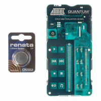
EVK2160A
Manufacturer Part Number
EVK2160A
Description
KIT EVAL FOR AT42QT2160-MMU
Manufacturer
Atmel
Series
Quantum, QTouch™r
Specifications of EVK2160A
Sensor Type
Touch, Capacitive
Sensing Range
8 Buttons/Keys, Slider
Interface
I²C
Voltage - Supply
1.8 V ~ 5.5 V
Embedded
No
Utilized Ic / Part
AT42QT2160
Silicon Manufacturer
Atmel
Silicon Core Number
AT42QT2160-MMU
Kit Application Type
Sensing - Touch / Proximity
Application Sub Type
Capacitive Touch
Kit Contents
Board CD Docs
Rohs Compliant
Yes
Lead Free Status / RoHS Status
Lead free / RoHS Compliant
Sensitivity
-
Lead Free Status / Rohs Status
Supplier Unconfirmed
Other names
427-1141
Available stocks
Company
Part Number
Manufacturer
Quantity
Price
Company:

Part Number:
EVK2160A
Manufacturer:
Atmel
Quantity:
135


4.5
4.6
4.7
9502A–AT42–07/08
Sample Resistors
Signal Levels
Matrix Series Resistors
Figure 4-4.
Note:
The sample resistors (Rs0...Rs1) are used to perform single-slope ADC conversion of the
acquired charge on each Cs capacitor. These resistors directly control acquisition gain; larger
values of Rs will proportionately increase signal gain. For most applications Rs should be 1MΩ.
Unused Y lines do not require an Rs resistor.
The signal values should normally be in the range of 200 to 750 counts with properly designed
key shapes and values of Rs. However, long adjacent runs of X and Y lines can also artificially
boost the signal values, and induce signal saturation; this is to be avoided. The X-to-Y coupling
should come mostly from intra-key electrode coupling, not from stray X-to-Y trace coupling.
The signal swing from the smallest finger touch should preferably exceed 8 counts, with 12
being a reasonable target. The signal threshold setting (NTHR) should be set to a value
guaranteed to be less than the signal swing caused by the smallest touch.
Increasing the burst length (BL) parameter will increase the signal strengths, as will increasing
the sampling resistor (Rs) values.
The X and Y matrix scan lines can use series resistors (Rx0...Rx7 and Ry0...Ry1 respectively)
for improved EMC performance
X drive lines require Rx in most cases to reduce edge rates and thus reduce RF emissions.
Values range from 1 kΩ to 20 kΩ, typically 1 kΩ.
Y lines need Ry to reduce EMC susceptibility problems and in some extreme cases, ESD.
Typical Y values are about 1 kΩ. Y resistors act to reduce noise susceptibility problems by
forming a natural low-pass filter with the Cs capacitors.
It is essential that the Rx and Ry resistors and Cs capacitors be placed very close to the chip.
Placing these parts more than a few millimeters away opens the circuit up to high frequency
interference problems (above 20 MHz) as the trace lengths between the components and the
chip start to act as RF antennae.
The upper limits of Rx and Ry are reached when the signal level and hence key sensitivity are
clearly reduced. The limits of Rx and Ry will depend on key geometry and stray capacitance,
and thus an oscilloscope is required to determine optimum values of both.
The Dwell time is a minimum of ~250ns - see
Drive Pulse Roll-off and Dwell Time
Dwell time
Y gate
X drive
(Figure 4-8 on page
Lost charge due to
inadequate settling
before end of dwell time
Section 4.7
15).
AT42QT2160
7
Related parts for EVK2160A
Image
Part Number
Description
Manufacturer
Datasheet
Request
R

Part Number:
Description:
DEV KIT FOR AVR/AVR32
Manufacturer:
Atmel
Datasheet:

Part Number:
Description:
INTERVAL AND WIPE/WASH WIPER CONTROL IC WITH DELAY
Manufacturer:
ATMEL Corporation
Datasheet:
Part Number:
Description:
Low-Voltage Voice-Switched IC for Hands-Free Operation
Manufacturer:
ATMEL Corporation
Datasheet:
Part Number:
Description:
MONOLITHIC INTEGRATED FEATUREPHONE CIRCUIT
Manufacturer:
ATMEL Corporation
Datasheet:
Part Number:
Description:
AM-FM Receiver IC U4255BM-M
Manufacturer:
ATMEL Corporation
Datasheet:
Part Number:
Description:
Monolithic Integrated Feature Phone Circuit
Manufacturer:
ATMEL Corporation
Datasheet:
Part Number:
Description:
Multistandard Video-IF and Quasi Parallel Sound Processing
Manufacturer:
ATMEL Corporation
Datasheet:
Part Number:
Description:
High-performance EE PLD
Manufacturer:
ATMEL Corporation
Datasheet:
Part Number:
Description:
8-bit Flash Microcontroller
Manufacturer:
ATMEL Corporation
Datasheet:
Part Number:
Description:
2-Wire Serial EEPROM
Manufacturer:
ATMEL Corporation
Datasheet: