EVK2160A Atmel, EVK2160A Datasheet - Page 5
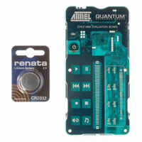
EVK2160A
Manufacturer Part Number
EVK2160A
Description
KIT EVAL FOR AT42QT2160-MMU
Manufacturer
Atmel
Series
Quantum, QTouch™r
Specifications of EVK2160A
Sensor Type
Touch, Capacitive
Sensing Range
8 Buttons/Keys, Slider
Interface
I²C
Voltage - Supply
1.8 V ~ 5.5 V
Embedded
No
Utilized Ic / Part
AT42QT2160
Silicon Manufacturer
Atmel
Silicon Core Number
AT42QT2160-MMU
Kit Application Type
Sensing - Touch / Proximity
Application Sub Type
Capacitive Touch
Kit Contents
Board CD Docs
Rohs Compliant
Yes
Lead Free Status / RoHS Status
Lead free / RoHS Compliant
Sensitivity
-
Lead Free Status / Rohs Status
Supplier Unconfirmed
Other names
427-1141
Available stocks
Company
Part Number
Manufacturer
Quantity
Price
Company:

Part Number:
EVK2160A
Manufacturer:
Atmel
Quantity:
135


4.2
4.3
4.4
9502A–AT42–07/08
Burst Paring
Cs Sample Capacitor Operation
Sample Capacitor Saturation
Keys that are disabled by setting their burst length to zero have their bursts removed from the
scan sequence to save scan time and thus power. The QT2160 operates on a fixed 16 ms cycle
and will go to sleep after all acquisitions and processing is done till the next 16ms cycle starts.
As a consequence, the fewer keys, the less power is consumed.
Cs capacitors (Cs0...Cs1) absorb charge from the key electrodes on the rising edge of each X
pulse. On each falling edge of X, the Y matrix line is clamped to ground to allow the electrode
and wiring charges to neutralize in preparation for the next pulse. With each X pulse charge
accumulates on Cs causing a staircase increase in its differential voltage.
After the burst completes, the device clamps the Y line to ground causing the opposite terminal
to go negative. The charge on Cs is then measured using an external resistor to ramp the
negative terminal upwards until a zero crossing is achieved. The time required to zero cross
becomes the measurement result.
The Cs capacitors should be connected as shown in
capacitors is not critical but 4.7 nF is recommended for most cases. They should be 10 percent
X7R ceramic. If the transverse capacitive coupling from X to Y is large enough the voltage on a
Cs capacitor can saturate, destroying gain. In such cases the burst length should be reduced
and/or the Cs value increased. See
If a Y line is not used its corresponding Cs capacitor may be omitted and the pins left floating.
Cs voltage saturation at a pin YnB is shown in
voltage at a YnB pin becomes more negative than -0.25V at the end of the burst. This
nonlinearity is caused by excessive voltage accumulation on Cs inducing conduction in the pin
protection diodes. This badly saturated signal destroys key gain and introduces a strong thermal
coefficient which can cause phantom detection. The cause of this is either from the burst length
being too long, the Cs value being too small, or the X-Y transfer coupling being too large.
Solutions include loosening up the key structure interleaving, more separation of the X and Y
lines on the PCB, increasing Cs, and decreasing the burst length.
Increasing Cs will make the part slower; decreasing burst length will make it less sensitive. A
better PCB layout and a looser key structure (up to a point) have no negative effects.
Cs voltages should be observed on an oscilloscope with the matrix layer bonded to the panel
material; if the Rs side of any Cs ramps more negative than -0.25 volts during any burst (not
counting overshoot spikes which are probe artifacts), there is a potential saturation problem.
Figure 4-2
distortion is caused by excessive stray capacitance coupling from the Y line to AC ground; for
example, from running too near and too far alongside a ground trace, ground plane, or other
traces. The excess coupling causes the charge-transfer effect to dissipate a significant portion of
the received charge from a key into the stray capacitance. This phenomenon is more subtle; it
can be best detected by increasing BL to a high count and watching what the waveform does as
it descends towards and below -0.25V. The waveform will appear deceptively straight, but it will
slowly start to flatten even before the -0.25V level is reached.
A correct waveform is shown in
substantially straight (ignoring the downward spikes).
shows a defective waveform similar to that of
Figure
Section
4-3. Note that the bottom edge of the bottom trace is
4.4.
Figure
Figure 4-8 on page
4-1. Saturation begins to occur when the
Figure
4-1, but in this case the
AT42QT2160
15. The value of these
5
Related parts for EVK2160A
Image
Part Number
Description
Manufacturer
Datasheet
Request
R

Part Number:
Description:
DEV KIT FOR AVR/AVR32
Manufacturer:
Atmel
Datasheet:

Part Number:
Description:
INTERVAL AND WIPE/WASH WIPER CONTROL IC WITH DELAY
Manufacturer:
ATMEL Corporation
Datasheet:
Part Number:
Description:
Low-Voltage Voice-Switched IC for Hands-Free Operation
Manufacturer:
ATMEL Corporation
Datasheet:
Part Number:
Description:
MONOLITHIC INTEGRATED FEATUREPHONE CIRCUIT
Manufacturer:
ATMEL Corporation
Datasheet:
Part Number:
Description:
AM-FM Receiver IC U4255BM-M
Manufacturer:
ATMEL Corporation
Datasheet:
Part Number:
Description:
Monolithic Integrated Feature Phone Circuit
Manufacturer:
ATMEL Corporation
Datasheet:
Part Number:
Description:
Multistandard Video-IF and Quasi Parallel Sound Processing
Manufacturer:
ATMEL Corporation
Datasheet:
Part Number:
Description:
High-performance EE PLD
Manufacturer:
ATMEL Corporation
Datasheet:
Part Number:
Description:
8-bit Flash Microcontroller
Manufacturer:
ATMEL Corporation
Datasheet:
Part Number:
Description:
2-Wire Serial EEPROM
Manufacturer:
ATMEL Corporation
Datasheet: