AD8330-EVALZ Analog Devices Inc, AD8330-EVALZ Datasheet - Page 24
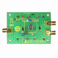
AD8330-EVALZ
Manufacturer Part Number
AD8330-EVALZ
Description
BOARD EVAL FOR AD8330
Manufacturer
Analog Devices Inc
Specifications of AD8330-EVALZ
Channels Per Ic
1 - Single
Amplifier Type
Variable Gain
Output Type
Differential, Rail-to-Rail
Slew Rate
1500 V/µs
-3db Bandwidth
150MHz
Operating Temperature
-40°C ~ 85°C
Current - Supply (main Ic)
20mA
Voltage - Supply, Single/dual (±)
2.7 V ~ 6 V
Board Type
Fully Populated
Utilized Ic / Part
AD8330
Silicon Manufacturer
Analog Devices
Application Sub Type
Variable Gain Amplifier
Kit Application Type
Amplifier
Silicon Core Number
AD8330
Kit Contents
Board
Lead Free Status / RoHS Status
Lead free / RoHS Compliant
Current - Output / Channel
-
Lead Free Status / RoHS Status
Lead free / RoHS Compliant, Lead free / RoHS Compliant


AD8330
Repeating the procedure,
The noise figure is the decibel representation of the noise factor,
N
However, this is equivalent to
Let V
source resistance. Using Equation 17 gives
Then, using the result from Equation 19 for a source resistance
of 1 kΩ, having a noise-spectral density of 4.08 nV/√Hz
produces
Finally, converting this to decibels using
Thus, the resultant noise figure in this example is 5.06 dB,
which is somewhat lower than the value shown in Figure 53 for
this operating condition.
Noise as a Function of V
The chief consequence of lowering the basic gain using V
that the current noise spectral density I
square root of the basic gain magnitude, G
Therefore, at the minimum basic gain of ×0, I
53.3 pA/√Hz. However, the noise figure rises to 17.2 db if it
is recalculated using the procedures in Equation 16 through
Equation 24.
Distortion Considerations
Continuously variable gain amplifiers invariably employ
nonlinear circuit elements; consequently, it is common for their
distortion to be higher than well-designed fixed gain amplifiers.
The translinear multiplier principles used in the AD8330, in
theory, yield extremely low distortion, a result of the funda-
mental linearization technique that is an inherent aspect of
these circuits.
FAC
, commonly defined as follows:
= 7.3 nV/√Hz
N
I
V
N
N
N
N
NSD
NSD
FIG
NOISE
FAC
FAC
FAC
FAC
be the voltage noise spectral density √kTRS due to the
= (3 pA/√Hz)(√G
= 10 log
=
=
=
=
=
_
SNR
IN
SNR
R
SNR
V
(
(
1
SNR
1
I
V
IN
R
=
kΩ
V
kΩ
at
S
SIG
NOISE
10
at
/
V
at
at
{
the
)
(N
V
(
)
(
{
4
(
output
. 4
NSD
7
the
R
NOISE
input
1 .
FAC
3 .
input
08
I
_
nV
IN
/
source
nV
)
(
nV/
R
_
/
I
IN
BN
DBS
pins
/
+
)
R
Hz
R
Hz
S
Hz
S
/
(
)
) (
}
R
)
2
)
/
I
+
=
V
+
. 1
NSD
3
R
79
NSD
pA
S
)
}
increases with the
BN
/
such that
NSD
Hz
rises to
)
2
(
1
kΩ
+
DBS
1
kΩ
(19)
(20)
(21)
(22)
(23)
(24)
(25)
is
Rev. E | Page 24 of 32
)
2
In practice, however, the effect of device mismatches and junc-
tion resistances in the core cell, and other mechanisms in its
supporting circuitry inevitably cause distortion, further aggravated
by other effects in the later output stages. Some of these effects
are very consistent from one sample to the next, while those due
to mismatches (causing predominantly even-order distortion
components) are quite variable. Where the highest linearity
(and lowest noise) is demanded, consider using one of the X-
AMP products such as the
(dual-channel), or
ultralow noise LNAs).
P1dB and V1dB
In addition to the nonlinearities that arise within the core of the
AD8330, at moderate output levels, another metric that is more
commonly stated for RF components that deliver appreciable
power to a load is the 1 dB compression point. This is defined
in a very specific manner: it is that point at which, with increasing
output level, the power delivered to the load eventually falls to a
value that is 1 dB lower than it would be for a perfectly linear
system. (Although this metric is sometimes called the 1 dB gain
compression point, it is important to note that this is not the
output level at which the incremental gain has fallen by 1 dB).
As shown in Figure 49, the output of the AD8330 limits quite
abruptly, and the gain drops sharply above the clipping level.
The output power, on the other hand, using an external resistive
load, R
waveform changes from the sinusoidal form of the test signal,
with an amplitude just below the clipping level, V
square wave of precisely the same amplitude. The change in
power over this range is from (V
is, a factor of 2, or 3 dB in power terms. It can be shown that for
an ideal limiting amplifier, the 1 dB compression point occurs
for an overdrive factor of 2 dB.
For example, if the AD8330 is driving a 150 Ω load and V
set to 2 V, the peak output is nominally ±4 V (as noted previously,
the actual value, when loaded. can differ because of a mismatch
between on-chip and external resistors), or 2.83 V rms for a sine
wave output that corresponds to a power of 53.3 mW, that is,
17.3 dBm in 150 Ω. Thus, the P1dB level, at 2 dB above
clipping, is 19.3 dBm.
Though not involving power transfer, it is sometimes useful
to state the V1dB, which is the output voltage (unloaded or
loaded) that is 2 dB above clipping for a sine waveform. In the
above example, this voltage is still 2.83 V rms, which can be
expressed as 9.04 dBV (0 dBV corresponds to a 1 V sine wave).
Thus, the V1dB is at 11.04 dBV.
L
, continues to increase. In the most extreme case, the
AD8332
AD603
(wideband dual-channel with
CLIP
(single-channel),
/√2)
2
/R
L
to (V
CLIP
CLIP
AD604
, to a
)
2
/R
L
, that
MAG
is
Related parts for AD8330-EVALZ
Image
Part Number
Description
Manufacturer
Datasheet
Request
R

Part Number:
Description:
BOARD EVAL FOR AD8330
Manufacturer:
Analog Devices Inc
Datasheet:

Part Number:
Description:
±1.7g Dual-Axis IMEMS Accelerometer Evaluation Board
Manufacturer:
Analog Devices Inc
Datasheet:

Part Number:
Description:
Inertial Sensor Evaluation System
Manufacturer:
Analog Devices Inc
Datasheet:
Part Number:
Description:
Manufacturer:
Analog Devices Inc
Datasheet:
Part Number:
Description:
Manufacturer:
Analog Devices Inc
Datasheet:
Part Number:
Description:
Manufacturer:
Analog Devices Inc
Datasheet:
Part Number:
Description:
Manufacturer:
Analog Devices Inc
Datasheet:
Part Number:
Description:
Manufacturer:
Analog Devices Inc
Datasheet:
Part Number:
Description:
Manufacturer:
Analog Devices Inc
Datasheet:
Part Number:
Description:
Manufacturer:
Analog Devices Inc
Datasheet:
Part Number:
Description:
Manufacturer:
Analog Devices Inc
Datasheet:
Part Number:
Description:
Manufacturer:
Analog Devices Inc
Datasheet:
Part Number:
Description:
Manufacturer:
Analog Devices Inc
Datasheet: