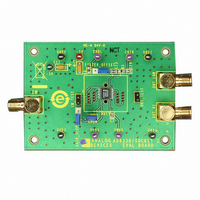
AD8330-EVALZ Analog Devices Inc, AD8330-EVALZ Datasheet - Page 19

AD8330-EVALZ
Manufacturer Part Number
AD8330-EVALZ
Description
BOARD EVAL FOR AD8330
Manufacturer
Analog Devices Inc
Specifications of AD8330-EVALZ
Channels Per Ic
1 - Single
Amplifier Type
Variable Gain
Output Type
Differential, Rail-to-Rail
Slew Rate
1500 V/µs
-3db Bandwidth
150MHz
Operating Temperature
-40°C ~ 85°C
Current - Supply (main Ic)
20mA
Voltage - Supply, Single/dual (±)
2.7 V ~ 6 V
Board Type
Fully Populated
Utilized Ic / Part
AD8330
Silicon Manufacturer
Analog Devices
Application Sub Type
Variable Gain Amplifier
Kit Application Type
Amplifier
Silicon Core Number
AD8330
Kit Contents
Board
Lead Free Status / RoHS Status
Lead free / RoHS Compliant
Current - Output / Channel
-
Lead Free Status / RoHS Status
Lead free / RoHS Compliant, Lead free / RoHS Compliant
Input Common-Mode Range and Rejection Ratio
Input Pin INHI and Pin INLO should be ac-coupled in most
applications to achieve the stated noise performance. In general,
when direct coupling is used, care must be taken in setting the
dc voltage level at these inputs, and particularly when minimizing
noise is critical. This objective is complicated by the fact that
the common-mode level varies with the basic gain voltage, V
Figure 55 shows this relationship for a supply voltage of 5 V, for
temperatures of −40°C, +25°C, and +85°C. Figure 56 shows the
input noise spectral density (R
mode voltage, for V
apparent that there is a broad range over which the noise is
unaffected by this dc level. The input CMRR is excellent (see
Figure 16).
Output Noise and Peak Swing
The output noise of the AD8330 is the input noise multiplied by
the overall gain, including any optional change to the voltage,
V
proportional to this voltage, which, at low gains and high values
of V
MAG
Figure 55. Common-Mode Voltage at Input Pins vs. V
MAG
, applied to Pin VMAG. The peak output swing is also
26
24
22
20
18
16
14
12
10
3.2
3.1
3.0
2.9
2.8
2.7
2.6
8
6
4
Figure 56. Input Noise vs. Common-Mode Input Voltage for
, affects the output noise.
0
0
0.4
SIMULATION
0.2
0.8
COMMON-MODE VOLTAGE AT INHI, INLO (V)
V
DBS
1.2
DBS
T = −40°C, + 25°C, and + 85°C
0.4
= 0.5 V, 0.6 V, 0.75 V, and 1.5 V
= 0.5 V, 0.6 V, 0.75 V, and 1.5 V. It is
1.6
0.6
2.0
S
V
2.4
= 0) vs. the input common-
DBS
0.8
(V)
2.8
1.0
3.2
T = +85°C
T = –40°C
V
T = +25°C
V
V
V
DBS
3.6
DBS
DBS
DBS
1.2
= 0.75V
= 0.5V
= 0.6V
= 1.5V
4.0
DBS
, for V
1.4
4.4
S
4.8
= 5 V,
1.6
Rev. E | Page 19 of 32
DBS
.
The scaling for V
For example, using a reduced value of V
all gain values by 6 dB, the peak output swing is ±1 V (differ-
entially) and the output noise spectral density evaluates to
102.5 nV/√Hz. The peak output swing is no different at full
gain, but the noise becomes
for R
The output noise for very small values of V
is not precise, partly because the small input offset associated
with this interface has a large effect on the gain.
Offset Compensation
The AD8330 includes an offset compensation feature that is
operational in the default condition (no connection to Pin OFST).
This loop introduces a high-pass filter function into the signal
path, whose −3 dB corner frequency is at
where:
C
R
maximum uncertainty of about ±20%.
This evaluates to
A small amount of peaking at this corner when using small
capacitor values can be avoided by adding a series resistor.
Useful combinations are C
C
f = 1 kHz; C
The offset compensation feature can be disabled simply by
grounding the OFST pin. This provides a dc-coupled signal
path, with no other effects on the overall ac response. Input
offsets must be externally nulled in this mode of operation, as
shown in Figure 58.
Effects of Loading on Gain and AC Response
The differential output impedance (R
quency response of the output stage is optimized for operation
with a certain load capacitance on each output pin (OPHI and
OPLO) to ground, in combination with a load resistance (R
directly across these pins. In the absence of these capacitances,
there is a small amount of peaking at the top extremity of the
ac response. Suitable combinations are: R
R
C
HP
INT
L
HP
L
= 150 Ω, C
= 50 pF.
is the external capacitance added from OFST to CNTR.
= 33 nF, R
is an internal resistance of approximately 480 Ω, having a
V
V
V
S
f
f
= 0 and V
OUT_PK
NOISE_OUT
NOISE_OUT
HPF
HPF
=
=
HP
330
= ±4 V
(
C
2
L
π
HP
= (85 + 70 V
HP
= 3.3 μF, R
= (0.1 + 0.32 V
= 25 pF; R
R
DBS
μ
= 10 Ω, f = 10 kHz; C
DBS
INT
1
(C
MAG
= 1.5 V, assuming an input noise of 5 nV/√Hz.
C
= 0 V is as follows:
HP
HP
in μF)
)
HP
L
HP
= 75 Ω, C
MAG
= 0 Ω, f = 100 Hz.
= 3 nF, R
MAG
) nV/√Hz
) μV/√Hz
L
O
HP
= 40 pF; or R
HP
) is 150 Ω, and the fre-
MAG
= 180 Ω, f = 100 kHz;
= 0.33 μF, R
MAG
L
= ∞, C
= 0.25 V that lowers
(at or below 15 mV)
L
= 12 pF;
L
AD8330
= 50 Ω,
HP
= 0 Ω,
L
(10)
(11)
(12)
)
(8)
(9)


