AD8330-EVALZ Analog Devices Inc, AD8330-EVALZ Datasheet - Page 14
AD8330-EVALZ
Manufacturer Part Number
AD8330-EVALZ
Description
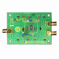
BOARD EVAL FOR AD8330
Manufacturer
Analog Devices Inc
Specifications of AD8330-EVALZ
Channels Per Ic
1 - Single
Amplifier Type
Variable Gain
Output Type
Differential, Rail-to-Rail
Slew Rate
1500 V/µs
-3db Bandwidth
150MHz
Operating Temperature
-40°C ~ 85°C
Current - Supply (main Ic)
20mA
Voltage - Supply, Single/dual (±)
2.7 V ~ 6 V
Board Type
Fully Populated
Utilized Ic / Part
AD8330
Silicon Manufacturer
Analog Devices
Application Sub Type
Variable Gain Amplifier
Kit Application Type
Amplifier
Silicon Core Number
AD8330
Kit Contents
Board
Lead Free Status / RoHS Status
Lead free / RoHS Compliant
Current - Output / Channel
-
Lead Free Status / RoHS Status
Lead free / RoHS Compliant, Lead free / RoHS Compliant


AD8330
THEORY OF OPERATION
CIRCUIT DESCRIPTION
Many monolithic variable gain amplifiers use techniques that
share common principles that are broadly classified as translinear.
This term refers to circuit cells whose functions depend directly
on the very predictable properties of bipolar junction transistors,
notably the linear dependence of their transconductance on collec-
tor current. Since the discovery of these cells in 1967, and their
commercial exploitation in products developed during the early
1970s, accurate wide bandwidth analog multipliers, dividers,
and variable gain amplifiers have invariably employed translinear
principles.
Although these techniques are well understood, the realization
of a high performance variable gain amplifier (VGA) requires
special technologies and attention to many subtle details in
its design. The AD8330 is fabricated on a proprietary silicon-
on-insulator, complementary bipolar IC process and draws
on decades of experience in developing many leading edge
products using translinear principles to provide an unprecedented
level of versatility.
Figure 45 shows a basic representative cell comprising just four
transistors. This, or a very closely related form, is at the heart
of most translinear multipliers, dividers, and VGAs. The key
concepts are as follows:
First, the ratio of the currents in the left-hand and right-hand
pairs of transistors is identical, represented by the modulation
factor, x, with values between −1 and +1. Second, the input
signal is arranged to modulate the fixed tail current, I
the variable value of x, introduced in the left-hand pair, to be
replicated in the right-hand pair, and, thus, generate the output
by modulating its nominally fixed tail current, I
current gain of this cell is exactly G = I
of variable bias current.
In practice, the realization of the full potential of this circuit
involves many other factors, but these three elementary ideas
remain essential.
By varying I
analog multiplier, exhibiting a linear relationship to both the
signal modulation factor (x) and this numerator current. On
the other hand, by varying I
is realized, having a hyperbolic gain function with respect to
the input factor, x, controlled by this denominator current. The
AD8330 exploits both modes of operation. However, because a
hyperbolic gain function is generally of less value than one in
which the decibel gain is a linear function of a control input, a
special interface is included to provide either increasing or
decreasing exponential control of I
N
, the overall function is that of a two-quadrant
D
, a two-quadrant analog divider
D
.
N
/I
D
over many decades
N
. Third, the
D
, to cause
Rev. E | Page 14 of 32
Overall Structure
Figure 46 shows a block schematic of the AD8330 locating the
key sections. More detailed descriptions of its structure and
features are provided throughout the Theory of Operation
section; however, Figure 46 provides a general overview of its
capabilities.
The VGA core contains a more elaborate version of the cell
shown in Figure 45. The current, I
(linear-in-decibels) through the decibel gain interface at
Pin VDBS and its local common, Pin CMGN. The gain span
(that is, the decibel difference between maximum and
minimum values) provided by this control function is slightly
more than 50 dB. The absolute gain from input to output is a
function of source and load impedance, and depends on the
voltage on a second gain control pin (VMAG), explained in the
Normal Operating Conditions section.
(1–x) I
INPUT IS xl
2
VPSI
INHI
INLO
MODE
D
E
Q1
VDBS
N
I
D
B
L
D
VGA CORE
Q2
BIAS AND
AD8330
DENOMINATOR
BIAS CURRENT
GAIN INTERFACE
(1–x) I
V
REF
Figure 46. Block Schematic
2
OFST
Figure 45. Basic Core
D
CMGN
G = I
+
N
OFFSET CONTROL
/I
D
BIAS CURRENT
CM MODE AND
–
VPOS
NUMERATOR
LOOP
AMPLIFIER
COMM
D
OUTPUT
STAGES
, is controlled exponentially
CONTROL
(1–x) I
OUTPUT
2
OUTPUT IS xl
N
Q3
C
VMAG
N
VPSO
OPHI
OPLO
CMOP
T
Q4
R
I
N
(1+x) I
N
2
N
Related parts for AD8330-EVALZ
Image
Part Number
Description
Manufacturer
Datasheet
Request
R

Part Number:
Description:
BOARD EVAL FOR AD8330
Manufacturer:
Analog Devices Inc
Datasheet:

Part Number:
Description:
±1.7g Dual-Axis IMEMS Accelerometer Evaluation Board
Manufacturer:
Analog Devices Inc
Datasheet:

Part Number:
Description:
Inertial Sensor Evaluation System
Manufacturer:
Analog Devices Inc
Datasheet:
Part Number:
Description:
Manufacturer:
Analog Devices Inc
Datasheet:
Part Number:
Description:
Manufacturer:
Analog Devices Inc
Datasheet:
Part Number:
Description:
Manufacturer:
Analog Devices Inc
Datasheet:
Part Number:
Description:
Manufacturer:
Analog Devices Inc
Datasheet:
Part Number:
Description:
Manufacturer:
Analog Devices Inc
Datasheet:
Part Number:
Description:
Manufacturer:
Analog Devices Inc
Datasheet:
Part Number:
Description:
Manufacturer:
Analog Devices Inc
Datasheet:
Part Number:
Description:
Manufacturer:
Analog Devices Inc
Datasheet:
Part Number:
Description:
Manufacturer:
Analog Devices Inc
Datasheet:
Part Number:
Description:
Manufacturer:
Analog Devices Inc
Datasheet: