AD8330-EVALZ Analog Devices Inc, AD8330-EVALZ Datasheet
AD8330-EVALZ
Specifications of AD8330-EVALZ


Related parts for AD8330-EVALZ


AD8330-EVALZ Summary of contents
Page 1
... Pin MODE, the gain decreases over the same range, with an opposite slope. A second gain control port is provided at the VMAG pin and allows the user to vary the numeric gain from a factor of 0.03 to 10. All the parameters of the AD8330 have low sensitivities to temperature and supply voltages. Rev. E Information furnished by Analog Devices is believed to be accurate and reliable ...
Page 2
... Evaluation Board ............................................................................ 28 General Description ................................................................... 28 Basic Operation .......................................................................... 28 Options ........................................................................................ 29 Measurement Setup.................................................................... 29 AD8330-EVALZ Board Design ................................................ 29 Outline Dimensions ....................................................................... 31 Ordering Guide .......................................................................... 32 10/04—Rev Rev. B Changes to Absolute Maximum Ratings ........................................ 4 Changes to Ordering Guide ............................................................. 4 Change to TPC 14 ............................................................................. 8 Note added to CP-16 Package ....................................................... 26 4/03— ...
Page 3
... AD8330 Unit V mV Ω pF nV/√ rms μV/° MHz V/μ nV/√Hz Ω dBc dBc mV rms kHz V kΩ ...
Page 4
... AD8330 Parameter CHIP ENABLE Logic Voltage for Full Shutdown Logic Voltage for Hibernate Mode Logic Voltage for Full Operation Current in Full Shutdown Current in Hibernate Mode 3 Minimum Time Delay POWER SUPPLY Supply Voltage Quiescent Current 1 The use of an input common-mode voltage significantly different from the internally set value is not recommended due to its effect on noise performance. ...
Page 5
... Exposure to absolute 0.62 W maximum rating conditions for extended periods may affect 1.67 W device reliability 200 mV S −65°C to +150°C ESD CAUTION 105.4°C/W 60°C/W 39°C/W −40°C to +85°C 300°C Rev Page AD8330 ...
Page 6
... OFST Used in Offset Control Modes. 16 ENBL Power Enable, Active High. EPAD Exposed Pad recommended that the pad be soldered to the ground plane. 12 VPSO 11 OPHI 10 OPLO 9 CMOP Table 4. 16-Lead QSOP Pin Function Descriptions Pin No DBS MAG Rev Page AD8330 TOP VIEW (Not to Scale ...
Page 7
... GAIN SCALING (mV/dB) Figure 8. Gain Slope Histogram 1.5V DBS 50 1.2V 40 0.9V 30 0. –10 –20 –30 –40 –50 100k 1M 10M FREQUENCY (Hz) AD8330 50MHz 1MHz 10MHz 1.4 1.6 100M 500M DBS ...
Page 8
... AD8330 4.8V MAG 40 1.52V 30 0.48V 20 0.15V 10 0.048V 0 0.015V –10 –20 –30 –40 100k 1M 10M FREQUENCY (Hz) Figure 10. Frequency Response for Various Values 0.75 V DBS 0.1V DBS 100k 1M 10M FREQUENCY (Hz) Figure 11. Group Delay vs. Frequency 0 –1 –2 –3 –4 –5 –6 –7 0 0.2 0.4 ...
Page 9
... T = +85° +25°C 0.2 0.4 0.6 0.8 1.0 1.2 1.4 V (V) DBS for Three Temperatures DBS f = 1MHz V = 0.125V MAG V = 0.5V MAG MAG 0.2 0.4 0.6 0.8 1.0 1.2 1.4 V (V) DBS for Three Values of V DBS AD8330 1.6 1.6 MAG ...
Page 10
... AD8330 1.5V DBS 100k 1M FREQUENCY (Hz) Figure 22. Input Referred Noise vs. Frequency 0.75V DBS p-p OUT – 1kΩ L –20 –30 –40 –50 –60 –70 –80 100k 1M FREQUENCY (Hz) Figure 23. Harmonic Distortion vs. Frequency 0.75V DBS p-p OUT – 1kΩ L –20 –30 –40 HD3 –50 –60 HD2 – ...
Page 11
... MAG 1.5 1.0 0.5 0 –0.5 –1.0 –1.5 –50 100M Figure 33. Full-Scale Transient Response, V Rev Page AD8330 f = 10MHz f = 50MHz 0.4 0.6 0.8 1.0 1.2 1.4 0.2 V (V) DBS Figure 31. OIP3 vs. V DBS f = 10MHz f = 50MHz 0.4 0.6 0.8 1.0 1.2 1 ...
Page 12
... AD8330 1.5 1.0 0.5 0 –0.5 –1.0 –1.5 –50 – TIME (ns) Figure 34. Full-Scale Transient Response MHz p-p OUT 1.5 1.0 0.5 0 –0.5 –1.0 –1.5 –50 – TIME (ns) Figure 35. Full-Scale Transient Response MHz p-p OUT 500mV C = 12pF 54pF 24pF L Figure 36. Transient Response vs. Various Load Capacitances ...
Page 13
... Rev Page +85°C 20 +25°C 18 –40° 0.2 0.4 0.6 0.8 1.0 1.2 V (V) DBS Figure 43. Supply Current vs Three Temperatures DBS 3.125V 2.5V 1.875V 3.125V 2.5V 1.875V Figure 44. CNTR Transient Response, Top: Input to CNTR, Bottom: V Single-Ended OUT AD8330 1.4 1.6 100ns ...
Page 14
... Overall Structure Figure 46 shows a block schematic of the AD8330 locating the , to cause key sections. More detailed descriptions of its structure and D features are provided throughout the Theory of Operation section; however, Figure 46 provides a general overview of its ...
Page 15
... V (it is actually ~2.75 V for DBS V), but the AD8330 is able to accept a forced common- S mode value, from zero with certain limitations. This S interface provides good common-mode rejection up to high frequencies (see Figure 16) and, thus, can be driven in either a single-sided or differential manner. However, operation using a differential drive is preferable, and this is assumed in the specifications, unless otherwise stated ...
Page 16
... Using this to calculate the output voltage, V from which it is apparent that the AD8330 implements a linear, two-quadrant multiplier with a bipolar V Because the AD8330 is a dc-coupled system, it can be used in many applications where a wideband two-quadrant multiplier function is required, from about 100 MHz from either input (V ...
Page 17
... This function might be needed, for example, in providing a variable drive to a power amplifier apparent from the foregoing sections that the AD8330 is both an IVGA and an OVGA in one package. This is an unusual and possibly confusing degree of versatility for a VGA; therefore, ...
Page 18
... S only one of these components is used, either the current (as in the AD8330) or the voltage. Then, even if the amplifier is perfect, the noise figure cannot be better than 3 dB. The 1 kΩ internal termination resistance would result in a minimum noise figure for an R noise-free ...
Page 19
... Figure 56. Input Noise vs. Common-Mode Input Voltage for V = 0.5 V, 0.6 V, 0.75 V, and 1.5 V DBS Output Noise and Peak Swing The output noise of the AD8330 is the input noise multiplied by the overall gain, including any optional change to the voltage applied to Pin VMAG. The peak output swing is also MAG ...
Page 20
... Figure 57; however, the Applications , at Pin INHI and section shows how a negative supply can optionally be used. The AD8330 is enabled by taking the ENBL pin to a logical high (14) (or, in all cases, the supply). The UP gain mode is enabled either by leaving the MODE pin unconnected or taking logical CMI high ...
Page 21
... Connections to the input and output pins are not shown in Figure 57 because of the many options that are available. When the AD8330 is used to drive an ADC, connect the OPHI and OPLO pins directly to the differential inputs of a suitable converter, such as an AD9214 adjustment is needed to this common- ...
Page 22
... These outputs are very symmetric, so the only effect of this choice is to select the desired polarity. However, when the frequency range of interest extends to the upper limits of the AD8330, a dummy resistor of the same value should be attached to the unused output. Figure 60 illustrates the ac gain and phase response for various loads and ...
Page 23
... Thus, when this pin is used to rapidly modulate the primary signal, some further experimentation with response optimization may be required. In general, the AD8330 is very tolerant of a wide range of loading conditions. Preserving Absolute Gain Although the AD8330 is not laser trimmed, its absolute gain calibration, based mainly on ratios, is very good ...
Page 24
... It can be shown that for an ideal limiting amplifier, the 1 dB compression point occurs for an overdrive factor of 2 dB. For example, if the AD8330 is driving a 150 Ω load and V set the peak output is nominally ±4 V (as noted previously, is DBS the actual value, when loaded ...
Page 25
... V of the nominal 1.1 V; variations ±20% in the AD8330 on-chip resistors change this voltage by only ±70 mV. With the connections shown in Figure 63, the AD9214 is able to receive an input p-p; the peak output of the AD8330 can be reduced if desired by adding a resistor 10Ω ENBL ...
Page 26
... Q1 CMOP The VMAG dynamic range from low frequencies to 2.7 GHz. 0.1µF This can increase to 110 dB using an AD8330 as a precondi tioner, provided the noise bandwidth is limited by an interstage 0.1µF low-pass or band-pass filter. The VGA also provides an input port that is easier to drive than the 200 Ω ...
Page 27
... AD8362 1 COMM ACOM 16 10µF 2 CHPF VREF 15 3 DECL VTGT 14 4 INHI VPOS 13 C FLT 3.6V 18nF 5 INLO VOUT 12 6 DECL VSET 11 7 PWDN ACOM 10 8 COMM CLPF TIME (ms) Rev Page AD8330 0.1µF VOUT 10µF 6.04kΩ 4.02kΩ ...
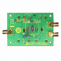
Page 28
... AD8330 EVALUATION BOARD GENERAL DESCRIPTION The AD8330-EVALZ is an easy-to-use accessory that enables a hands-on evaluation of the AD8330 variable gain amplifier (VGA). It includes test pins for connections to all of the functional device inputs. Figure full size photograph of the board. Figure 69. Photograph of the AD8330 Evaluation Board 10µ ...
Page 29
... OUT_LO can also be used, but the user may need to account for load capacitance effects. AD8330-EVALZ BOARD DESIGN The AD8330-EVALZ is a 4-layer design for maximum ground- plane area. The evaluation board side silkscreen and wiring patterns are shown in Figure 72 through Figure 77. ...
Page 30
... AD8330 Figure 72. Component-Side Silkscreen Figure 73. Component-Side Wiring Figure 74. Ground Plane Figure 75. Wiring-Side Silkscreen Figure 76. Wiring-Side Pattern Figure 77. Inner Layer 2 Rev Page ...
Page 31
... SEATING 0.010 BSC 0.008 PLANE 0.006 0.004 COMPLIANT TO JEDEC STANDARDS MO-137-AB Figure 79. 16-Lead Shrink Small Outline Package [QSOP] (RQ-16) Dimensions shown in inches Rev Page 0.50 0.40 0. 1.50 SQ 1.35 PAD 4 5 0.25 MIN 8° 0° 0.050 0.016 AD8330 ...
Page 32
... AD8330ARQZ −40°C to +85°C AD8330ARQZ-RL −40°C to +85°C AD8330ARQZ-R7 −40°C to +85°C AD8330-EVALZ RoHS Compliant Part. ©2003–2010 Analog Devices, Inc. All rights reserved. Trademarks and registered trademarks are the property of their respective owners. Package Description 16-Lead LFCSP_VQ ...