RDK-193 Power Integrations, RDK-193 Datasheet - Page 9
RDK-193
Manufacturer Part Number
RDK-193
Description
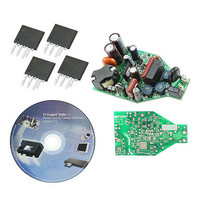
KIT REF DESIGN FOR LNK403EG
Manufacturer
Power Integrations
Type
Power Factor Correctionr
Specifications of RDK-193
Current - Output / Channel
330mA
Outputs And Type
1, Non-Isolated
Voltage - Output
21V
Features
Dimmable with Standard TRIAC Dimmer, Power Factor Correction
Voltage - Input
90 ~ 265VAC
Utilized Ic / Part
LNK403EG
Input Voltage
90 V to 265 V
Output Voltage
21 V
Product
Power Management Modules
Lead Free Status / RoHS Status
Lead free / RoHS Compliant
For Use With/related Products
LNK403EG
Other names
596-1307
Available stocks
Company
Part Number
Manufacturer
Quantity
Price
Company:

Part Number:
RDK-193
Manufacturer:
Power Integrations
Quantity:
135


09-Jun-10
RDR-193 7 W PAR20 LED Driver Using LNK403EG
4 Circuit Description
The LinkSwitch-PH device is a controller and integrated 725 V MOSFET intended for use
in LED driver applications. The LinkSwitch-PH is configured for use in a single-stage
continuous conduction mode Flyback topology and provides a primary side regulated
constant current output while maintaining high power factor from the AC input.
4.1 Input Filtering
Fuse F1 fuses the input and BR1 rectifies the AC line voltage. Inductor L1-L3, C2, R2,
and R3 form EMI filter with C7 Y capacitor. Small bulk capacitor C3 is required for a low
impedance path for the primary switching current. A low value of capacitance is
necessary to maintain a power factor of greater than 0.9.
4.2 LinkSwitch-PH Primary
Diode D6 and C8 detect the peak AC line voltage. This voltage is converted to a current
into the V pin via R4 and R7. This current is also used by the device to set the input
over/undervoltage protection thresholds. The V pin current and the FB pin current are
used internally to control the average output LED current. TRIAC phase-angle dimming
applications require 49.9 k resistors on the R pin and 4 M on the V pin to provide a
linear relationship between input voltage and the output current. Resistor R4 also sets the
internal references to select the brown-in and brown-out and input overvoltage protection
thresholds.
Diode D1 and VR1 clamp the drain voltage to a safe level from the leakage inductance
voltage spike. Diode D5 is necessary to prevent reverse current from flowing through the
LinkSwitch-PH device.
4.3 Bias and Output Rectification
Diode D3, C6, R5, R9 and R18 create the primary bias supply. This voltage created from
the transformer bias winding supplies bias current into the BYPASS pin through D4 and
R10. Capacitor C12 is the main supply for the LinkSwitch-PH, which is charged to ~6 V at
start-up from an internal high-voltage current source tied to the device DRAIN pin. A
current proportional to the output voltage from the primary bias winding is fed into the
FEEDBACK pin through R15. Diode D2 rectifies the secondary winding while capacitors
C4 and C5 filter the output. Diode D8, R24, C14, VR3, C15, R23, and Q2 provide an
open load overvoltage protection function. This protects output capacitors, C4 and C5
from excessive voltage should the load be disconnected.
4.4 TRIAC Phase Dimming Control
Components R12, R13, R20, R17, D7, Q1, C13, VR2, and Q3 in conjunction with R16
reduce the inrush current when the TRIAC dimmer turns on. This circuit allows the inrush
current to flow through R16 for the first 2.4 ms at 115 VAC (1.2 ms at 230 VAC) of the
TRIAC conduction. After approximately 2.4 ms, Q3 turns on and shorts R16. This keeps
the power dissipation on R16 low. Resistor R12, R13, R20 and C13 provide a 2.4 ms
Power Integrations
Tel: +1 408 414 9200 Fax: +1 408 414 9201
Page 9 of 41
www.powerint.com
Related parts for RDK-193
Image
Part Number
Description
Manufacturer
Datasheet
Request
R

Part Number:
Description:
KIT REF DESIGN FOR LNK457D
Manufacturer:
Power Integrations
Datasheet:

Part Number:
Description:
REFERENCE DESIGN LINKSWITCH-PH
Manufacturer:
Power Integrations
Datasheet:

Part Number:
Description:
KIT REF DESIGN FOR LNK406EG
Manufacturer:
Power Integrations
Datasheet:

Part Number:
Description:
KIT REF DESIGN LINKSWITCH-CV
Manufacturer:
Power Integrations
Datasheet:

Part Number:
Description:
KIT REF DESIGN LINKSWITCH 2
Manufacturer:
Power Integrations
Datasheet:

Part Number:
Description:
Specifications: Family: Eval Boards - DC/DC & AC/DC (Off-Line) SMPS ; Series: HiperLCS™ ; Main Purpose: DC/DC, Step Down ; Outputs and Type: 1, Isolated ; Power - Output: 150W ; Voltage - Output: 24V ; Current - Output: 6.25A ; Voltage - Input:
Manufacturer:
Power Integrations, Inc.
Datasheet:

Part Number:
Description:
KIT DESIGN REF TINYSWITCH-III
Manufacturer:
Power Integrations
Datasheet:

Part Number:
Description:
KIT DESIGN REF LINKSWITCH LP
Manufacturer:
Power Integrations
Datasheet:

Part Number:
Description:
KIT REF DESIGN LED LINKSWITCH TN
Manufacturer:
Power Integrations
Datasheet:
Part Number:
Description:
KIT REF DESIGN PG LINKSWITCH-II
Manufacturer:
Power Integrations
Datasheet:
Part Number:
Description:
REFERENCE DESIGN LINKSWITCH-PL
Manufacturer:
Power Integrations
Datasheet:
Part Number:
Description:
REFERENCE DESIGN LINKSWITCH-PH
Manufacturer:
Power Integrations
Datasheet:

Part Number:
Description:
KIT REF DESIGN 36-72W MOTOR DRVR
Manufacturer:
Power Integrations
Datasheet:
Part Number:
Description:
Specifications: Manufacturer: Power Integrations ; Output Voltage: 380 VDC ; Input / Supply Voltage (Max): 264 VAC ; Input / Supply Voltage (Min): 90 VAC ; Mounting Style: Through Hole ; Output Current: 0.913 A ; Output Power: 347 W
Manufacturer:
Power Integrations, Inc.

Part Number:
Description:
KIT REF DESIGN TOP HX FOR TOP258
Manufacturer:
Power Integrations
Datasheet: