NCP1028LEDGEVB ON Semiconductor, NCP1028LEDGEVB Datasheet - Page 5
NCP1028LEDGEVB
Manufacturer Part Number
NCP1028LEDGEVB
Description
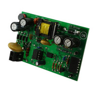
EVAL BOARD FOR NCP1028LEDG
Manufacturer
ON Semiconductor
Specifications of NCP1028LEDGEVB
Design Resources
NCP1028LEDGEVB BOM CP1028LEDGEVB Gerber Files NCP1028LED EVB Schematic
Current - Output / Channel
720mA
Outputs And Type
1, Isolated
Voltage - Output
18V
Voltage - Input
90 ~ 265VAC
Utilized Ic / Part
NCP1028
Core Chip
NCP1028
Topology
Flyback
No. Of Outputs
1
Output Current
720mA
Output Voltage
18V
Development Tool Type
Hardware - Eval/Demo Board
Leaded Process Compatible
Yes
Mcu Supported Families
NCP1028
Rohs Compliant
Yes
Lead Free Status / RoHS Status
Lead free / RoHS Compliant
Features
-
Lead Free Status / Rohs Status
Lead free / RoHS Compliant
For Use With/related Products
NCP1028LEDG
Other names
NCP1028LEDGEVBOS


3. See characterization curves for full temperature span evolution.
4. The final switch current is: Ipeak_2X_CS + Tprop x Vin / Lp, with Vin the input voltage and Lp the primary inductor in a flyback.
5. Oscillator frequency is measured with disabled jittering.
Maximum Internal Current Setpoint, Pin 4 Open, T
F
Final Switch Current with a Primary Slope of 200 mA/ms,
F
Maximum Internal Current Setpoint, Pin 4 Open, T
F
Final Switch Current with a Primary Slope of 200 mA/ms,
F
Setpoint Decrease for a Pin 7 Injected Current of 40 mA, T
Voltage Level in Pin 7 at which OPP Starts to Operate
Soft-Start Duration
Propagation Delay from Current Detection to Drain OFF State
Leading Edge Blanking Duration
Oscillation Frequency (Note 5)
65 kHz Version, T
Oscillation Frequency (Note 5)
100 kHz Version, T
Frequency Jittering in Percentage of f
Jittering Swing Frequency
Maximum Duty Cycle
Internal Pullup Resistor
Ramp Compensation Level on Pin 1 – Rramp = 100 kW
Internal Skip Mode Level, in Percentage of Maximum Peak Current
Brown-Out Level
Brown-Out Hysteresis Current, T
Brown-Out Hysteresis Current, T
Fault Validation further to Error Flag Assertion
OFF Phase in Fault Mode
Latching Voltage on Brown-Out Pin
Latch Input Integrating Filter Time Constant
Temperature Shutdown
Hysteresis in Shutdown
ELECTRICAL CHARACTERISTICS (continued)
Max T
CURRENT COMPARATOR
INTERNAL OSCILLATOR
FEEDBACK SECTION
SKIP CYCLE GENERATION
PROTECTIONS
TEMPERATURE MANAGEMENT
SW
SW
SW
SW
= 65 kHz (Note 3)
= 65 kHz (Note 4)
= 100 kHz (Note 3)
= 100 kHz (Note 4)
J
= 150°C, V
J
CC
J
= 25°C
= 25°C
= 8.0 V, unless otherwise noted.)
Characteristic
J
J
= 25°C (Note 3)
= 0°C to 125°C
OSC
J
J
= 25°C,
= 25°C,
(For typical values T
J
http://onsemi.com
= 25°C
NCP1028
5
J
Pin
-
-
-
-
7
7
-
-
-
-
-
-
-
-
4
2
-
3
3
3
-
-
3
3
-
-
= 25°C, for min/max values T
Ipeak_27_SW_
Ipeak_27_SW_
Ipeak_27_CS_
Ipeak_27_CS_
IOPPtripV
TimerOFF
IBOhyste
IBOhyste
TimerON
TdelBOL
Symbol
fswing
Rlevel
Vlatch
Dmax
100 k
100 k
IOPP
Rupp
T
T
f
VBO
f
f
Iskip
TSD
65 k
65 k
T
OSC
OSC
Jitter
prop
LEB
SS
-
58.5
3.15
Min
720
720
510
160
90
74
10
40
-
-
-
-
-
-
-
-
-
-
-
-
-
-
-
-
J
= 0°C to +125°C,
"6.0
2.75
11.5
Typ
800
820
800
820
100
200
100
300
570
440
1.5
1.0
3.5
23
65
80
16
25
10
55
20
40
-
Max
71.5
3.85
880
880
110
620
87
13
-
-
-
-
-
-
-
-
-
-
-
-
-
-
-
-
-
-
Unit
kHz
kHz
mA
mA
mA
mA
mV
ms
kW
ms
ms
Hz
mA
mA
ns
ns
ms
°C
°C
%
%
%
%
V
V
V
Related parts for NCP1028LEDGEVB
Image
Part Number
Description
Manufacturer
Datasheet
Request
R

Part Number:
Description:
Low Dropout Linear Regulator Controller
Manufacturer:
ON Semiconductor
Datasheet:

Part Number:
Description:
EVAL BOARD FOR NCP102MBG
Manufacturer:
ON Semiconductor
Datasheet:
Part Number:
Description:
ON Semiconductor [VOLTAGE REGULATOR]
Manufacturer:
ON Semiconductor
Datasheet:
Part Number:
Description:
357-036-542-201 CARDEDGE 36POS DL .156 BLK LOPRO
Manufacturer:
ON Semiconductor
Datasheet:
Part Number:
Description:
357-036-542-201 CARDEDGE 36POS DL .156 BLK LOPRO
Manufacturer:
ON Semiconductor
Datasheet:
Part Number:
Description:
357-036-542-201 CARDEDGE 36POS DL .156 BLK LOPRO
Manufacturer:
ON Semiconductor
Datasheet:
Part Number:
Description:
357-036-542-201 CARDEDGE 36POS DL .156 BLK LOPRO
Manufacturer:
ON Semiconductor
Datasheet:
Part Number:
Description:
357-036-542-201 CARDEDGE 36POS DL .156 BLK LOPRO
Manufacturer:
ON Semiconductor
Datasheet:
Part Number:
Description:
357-036-542-201 CARDEDGE 36POS DL .156 BLK LOPRO
Manufacturer:
ON Semiconductor
Datasheet:
Part Number:
Description:
357-036-542-201 CARDEDGE 36POS DL .156 BLK LOPRO
Manufacturer:
ON Semiconductor
Datasheet:
Part Number:
Description:
357-036-542-201 CARDEDGE 36POS DL .156 BLK LOPRO
Manufacturer:
ON Semiconductor
Datasheet:
Part Number:
Description:
357-036-542-201 CARDEDGE 36POS DL .156 BLK LOPRO
Manufacturer:
ON Semiconductor
Datasheet:
Part Number:
Description:
357-036-542-201 CARDEDGE 36POS DL .156 BLK LOPRO
Manufacturer:
ON Semiconductor
Datasheet:
Part Number:
Description:
Manufacturer:
ON Semiconductor
Datasheet: