NCP1028LEDGEVB ON Semiconductor, NCP1028LEDGEVB Datasheet
NCP1028LEDGEVB
Specifications of NCP1028LEDGEVB


Related parts for NCP1028LEDGEVB


NCP1028LEDGEVB Summary of contents
Page 1
... Reference 230 VAC NCP1028 - 5 *Typical values, open-frame, 65 kHz version, R **For additional information on our Pb-Free strategy and soldering details, please download the ON Semiconductor Soldering and Mounting Techniques Reference Manual, SOLDERRM/D. © Semiconductor Components Industries, LLC, 2007 December, 2007 - Rev 5 25°C DS(on) J Ramp Comp ...
Page 2
VAC *Optional component PIN FUNCTION DESCRIPTION Pin No. Symbol Function 1 V Powers the Internal CC Circuitry 2 Ramp Comp. Ramp Compensation in CCM 3 Brown-Out Brown-Out and Latchoff Input 4 FB Feedback Signal Input 5 Drain Drain ...
Page 3
V CC Vclamp Vlatch V < Reset IBO + VBO 65 kHz or 100 kHz CLOCK Jittering V dd Icomp Ramp Comp. 25 Skip + ...
Page 4
MAXIMUM RATINGS Rating Power Supply Voltage on all Pins, Except Pin 5 (Drain) Drain Voltage Drain Current Peak During Transformer Saturation Maximum Current into Pin 1 when Activating the 8.7 V Active Clamp Thermal Resistance, Junction-to-Air – PDIP7 Thermal Resistance, ...
Page 5
ELECTRICAL CHARACTERISTICS (continued) Max T = 150° 8.0 V, unless otherwise noted Characteristic CURRENT COMPARATOR Maximum Internal Current Setpoint, Pin 4 Open kHz (Note 3) SW Final Switch Current with a Primary ...
Page 6
TEMPERATURE (°C) Figure 4. 1.8 1.6 1.4 1.2 1.0 ...
Page 7
TEMPERATURE (°C) Figure 8. 120 100 -40 - TEMPERATURE (°C) Figure 10. 610 600 590 ...
Page 8
TEMPERATURE (°C) Figure 14. 3.8 3.7 3.6 3.5 3.4 3.3 3.2 - TEMPERATURE (°C) Figure 16. 400 380 360 340 ...
Page 9
TEMPERATURE (°C) Figure 20. 100% 90% 80% 70% 60% 50% 40% 30% 20% 10 Figure 22. Ipeak Reduction = F(lopp, @ ...
Page 10
... V–5.8 W Power Switch Circuit: Due to ON Semiconductor Very High Voltage Integrated Circuit technology, the circuit hosts a high-voltage power switch circuit featuring a 5 25°C. This value lets the designer build power supply operated on universal mains as long as sufficient copper area exists to lower the junction-to-ambient thermal resistance ...
Page 11
Startup Sequence The NCP1028 includes a high-voltage startup circuitry, directly deriving current from the bulk line to charge the Vbulk Figure 23. Internal Arrangement of the Startup Circuitry When the power supply is ...
Page 12
Figure 24. A typical startup sequence showing the V Suppose our power supply takes the output voltage to its target value. We know that the switcher consumption is around 2 can calculate the amount ...
Page 13
Fault Condition – Output Short-Circuit As soon as V reaches VCC CC ON internally enabled. If everything is correct, the auxiliary winding increases the voltage on the V voltage rises. During the start-sequence, the controller smoothly ramps up the peak ...
Page 14
In Figure 26, one can see that the V testifying for a badly coupled power secondary and primary auxiliary windings. Some situations exist where an output short-circuit make the auxiliary winding collapse Figure 27. The auxiliary winding collapses in presence ...
Page 15
Fault Condition – Output Too Low This particular mode of operation occurs when the feedback is ensured by a two-loop control imposing either constant output voltage (CV) or constant output current (CC), for instance in a battery charger ...
Page 16
Fault Condition – Low Input Voltage The NCP1028 includes a brown-out circuitry able to protect the power supply in case of low input voltage conditions. Figure 29 shows how internally the NCP1028 monitors the voltage image of the bulk capacitor. ...
Page 17
The bridge power dissipation is 330 nominal high-line operation. Figure 29b simulation result confirms our calculations. Figure 30 describes signal variations during a brown-out condition. Please note that output pulses only reappear Figure 30. Signal Evolution During ...
Page 18
Vout Figure 31. Adding a comparator on the BO pin offers a way to latch-off the controller. In Figure 31 blocked and does not bother the BO measurement as long as the NTC and the optocoupler are not ...
Page 19
Designing the Auxiliary Winding A NCP1028 internal arrangement clamps the voltage applied on the V pin. It uses an active shunt circuitry as CC shown on Figure 33. Care must be taken to avoid injecting too much current when the ...
Page 20
Figure 34. The burst frequency becomes so low that it is difficult to keep an adequate level on the auxiliary Over Power Compensation Over Power Compensation or Protection (OPP) represents a way to limit ...
Page 21
This difference might not be seen as a problem, but some design specifications impose stringent conditions on the maximum output current capability, regardless the line input. Hence the need for an OPP input… Since we want to limit the power ...
Page 22
The principle consists in selecting the RR resistor, connected from pin 2 to ground, to impose a current the transistor collector. Figure 38. Maximum Peak Current Setpoint Variations versus Ramp Compensation The equation to get the right compensation level is ...
Page 23
Jittering Frequency jittering is a method used to soften the EMI signature by spreading the energy in the vicinity of the main switching component. The NCP1028 offers a "6% deviation of the nominal switching frequency. The sweep 61.1kHz Figure 40. ...
Page 24
V/3.0 A Universal Mains Power Supply Due to its low R , the NCP1028 can be used in DS(on) universal mains SMPS continuous power, provided that the chip power dissipation is well under control. ...
Page 25
Large K: approaching BCM where the rms losses are the worse, but smaller inductance, leading to a better leakage inductance. From Equation 16 factor of 0.8 (40% ripple), gives an inductance of: 0.49) 2 (120 L + ...
Page 26
V above the reflected clamp value The diode needs fast one and out f an MUR160 represents a good choice. One major drawback of the RCD network lies ...
Page 27
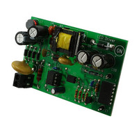
NCP1028 Figure 46. 5.0 V-3.0 A Universal Mains Power Supply http://onsemi.com 27 ...
Page 28
Transformer Specifications: Vout = 5.0 V/3.0 A Vaux = 20 V/ 3.8 mH Ip, rms = 280 mA Ip, max = 800 mA Isec, rms = 5.0 A Fsw = 65 kHz Np:Nsec = 1 : 0.052 ...
Page 29
... SCILLC is an Equal Opportunity/Affirmative Action Employer. This literature is subject to all applicable copyright laws and is not for resale in any manner. PUBLICATION ORDERING INFORMATION LITERATURE FULFILLMENT: Literature Distribution Center for ON Semiconductor P.O. Box 5163, Denver, Colorado 80217 USA Phone: 303-675-2175 or 800-344-3860 Toll Free USA/Canada ...