NCP1028LEDGEVB ON Semiconductor, NCP1028LEDGEVB Datasheet - Page 4
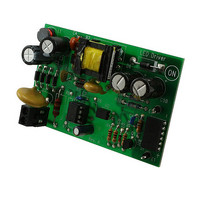
NCP1028LEDGEVB
Manufacturer Part Number
NCP1028LEDGEVB
Description
EVAL BOARD FOR NCP1028LEDG
Manufacturer
ON Semiconductor
Specifications of NCP1028LEDGEVB
Design Resources
NCP1028LEDGEVB BOM CP1028LEDGEVB Gerber Files NCP1028LED EVB Schematic
Current - Output / Channel
720mA
Outputs And Type
1, Isolated
Voltage - Output
18V
Voltage - Input
90 ~ 265VAC
Utilized Ic / Part
NCP1028
Core Chip
NCP1028
Topology
Flyback
No. Of Outputs
1
Output Current
720mA
Output Voltage
18V
Development Tool Type
Hardware - Eval/Demo Board
Leaded Process Compatible
Yes
Mcu Supported Families
NCP1028
Rohs Compliant
Yes
Lead Free Status / RoHS Status
Lead free / RoHS Compliant
Features
-
Lead Free Status / Rohs Status
Lead free / RoHS Compliant
For Use With/related Products
NCP1028LEDG
Other names
NCP1028LEDGEVBOS


Stresses exceeding Maximum Ratings may damage the device. Maximum Ratings are stress ratings only. Functional operation above the
Recommended Operating Conditions is not implied. Extended exposure to stresses above the Recommended Operating Conditions may affect
device reliability.
1. This device series contains ESD protection and exceeds the following tests:
2. This device contains latchup protection and exceeds 100 mA per JEDEC Standard JESD78.
Power Supply Voltage on all Pins, Except Pin 5 (Drain)
Drain Voltage
Maximum Current into Pin 1 when Activating the 8.7 V Active Clamp
Thermal Resistance, Junction-to-Air – PDIP7
Thermal Resistance, Junction-to-Air – PDIP7 with 1.0 cm@ of 35 m Copper Area
Maximum Junction Temperature
Storage Temperature Range
ESD Capability, Human Body Model (HBM) (All Pins Except HV)
ESD Capability, Machine Model (MM)
V
V
Hysteresis between VCC
Offset Voltage above VCC
V
Internal IC Consumption, MOSFET Switching at
Power Switch Circuit On-State Resistance
NCP1028 (Id = 100 mA)
Power Switch Circuit and Startup Breakdown Voltage
(ID
Power Switch and Startup Breakdown Voltage Off-State
Leakage Current
Switching Characteristics (RL = 50 W, Vds Set for
Idrain = 0.7 x Ilim)
High-Voltage Current Source, V
High-Voltage Current Source, V
V
MAXIMUM RATINGS
ELECTRICAL CHARACTERISTICS
V
SUPPLY SECTION AND V
POWER SWITCH CIRCUIT
INTERNAL STARTUP CURRENT SOURCE
Drain Current Peak During Transformer Saturation
CC
CC
CC
CC
CC
(off)
T
T
T
T
Turn-on Time (90%-10%)
Turn-off Time (10%-90%)
Human Body Model 2000 V per Mil-Std-883, Method 3015.
Machine Model Method 200 V.
Increasing Level at which the Switcher Starts to Operate
Decreasing Level at which the Switcher Stops Operation
Voltage at which the Internal Latch is Reset
Transition Level for IC1 to IC2 Toggling Point
= 8.0 V, unless otherwise noted.)
J
J
J
J
= 25°C
= 125°C
= 25°C (Vds = 700 V)
= 125°C (Vds = 700 V)
= 120 mA, T
J
= 25°C)
ON
ON
CC
and VCC
Characteristic
at which the Internal Clamp Activates
MANAGEMENT
CC
CC
= VCC
= 0
Rating
(min)
ON
(For typical values T
– 200 mV
65 kHz or 100 kHz
http://onsemi.com
J
NCP1028
= 25°C, for min/max values T
4
Pin
1
1
-
1
1
1
5
5
5
5
5
5
1
1
1
Idss(OFF)
Symbol
VCC
IDS(pk)
VCC
VCC
VCC
BVdss
TJ
Symbol
I_V
VCC
R
R
R
BVdss
V
V
ICC1
DS(on)
IC1
IC2
qJA
qJA
MAX
CCTh
CC
-
-
-
t
t
on
off
CC
clamp
hyste
J
(min)
reset
ON
= 0°C to +125°C, Max T
Min
140
700
350
7.9
6.7
3.5
-
-
-
-
-
-
-
-
-
-
-60 to +150
-0.3 to 700
-0.3 to 10
Value
100
150
200
2.0
1.8
15
75
Typ
200
650
8.5
7.2
1.2
4.0
1.4
5.8
9.8
6.0
1.3
50
30
35
35
-
J
= 150°C,
Max
300
900
8.9
7.9
1.9
7.0
8.0
11
-
-
-
-
-
-
-
-
°C/W
°C/W
Unit
mA
°C
°C
kV
V
V
A
V
Unit
mV
mA
mA
mA
mA
ns
ns
W
V
V
V
V
V
V
Related parts for NCP1028LEDGEVB
Image
Part Number
Description
Manufacturer
Datasheet
Request
R

Part Number:
Description:
Low Dropout Linear Regulator Controller
Manufacturer:
ON Semiconductor
Datasheet:

Part Number:
Description:
EVAL BOARD FOR NCP102MBG
Manufacturer:
ON Semiconductor
Datasheet:
Part Number:
Description:
ON Semiconductor [VOLTAGE REGULATOR]
Manufacturer:
ON Semiconductor
Datasheet:
Part Number:
Description:
357-036-542-201 CARDEDGE 36POS DL .156 BLK LOPRO
Manufacturer:
ON Semiconductor
Datasheet:
Part Number:
Description:
357-036-542-201 CARDEDGE 36POS DL .156 BLK LOPRO
Manufacturer:
ON Semiconductor
Datasheet:
Part Number:
Description:
357-036-542-201 CARDEDGE 36POS DL .156 BLK LOPRO
Manufacturer:
ON Semiconductor
Datasheet:
Part Number:
Description:
357-036-542-201 CARDEDGE 36POS DL .156 BLK LOPRO
Manufacturer:
ON Semiconductor
Datasheet:
Part Number:
Description:
357-036-542-201 CARDEDGE 36POS DL .156 BLK LOPRO
Manufacturer:
ON Semiconductor
Datasheet:
Part Number:
Description:
357-036-542-201 CARDEDGE 36POS DL .156 BLK LOPRO
Manufacturer:
ON Semiconductor
Datasheet:
Part Number:
Description:
357-036-542-201 CARDEDGE 36POS DL .156 BLK LOPRO
Manufacturer:
ON Semiconductor
Datasheet:
Part Number:
Description:
357-036-542-201 CARDEDGE 36POS DL .156 BLK LOPRO
Manufacturer:
ON Semiconductor
Datasheet:
Part Number:
Description:
357-036-542-201 CARDEDGE 36POS DL .156 BLK LOPRO
Manufacturer:
ON Semiconductor
Datasheet:
Part Number:
Description:
357-036-542-201 CARDEDGE 36POS DL .156 BLK LOPRO
Manufacturer:
ON Semiconductor
Datasheet:
Part Number:
Description:
Manufacturer:
ON Semiconductor
Datasheet: