EVAL-AD5379EBZ Analog Devices Inc, EVAL-AD5379EBZ Datasheet - Page 5
EVAL-AD5379EBZ
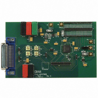
Manufacturer Part Number
EVAL-AD5379EBZ
Description
BOARD EVALUATION FOR AD5379
Manufacturer
Analog Devices Inc
Datasheet
1.AD5379ABCZ.pdf
(28 pages)
Specifications of EVAL-AD5379EBZ
Number Of Dac's
40
Number Of Bits
14
Outputs And Type
40, Single Ended
Sampling Rate (per Second)
50k
Data Interface
Serial, Parallel
Settling Time
20µs
Dac Type
Voltage
Voltage Supply Source
Analog and Digital, Dual ±
Operating Temperature
-40°C ~ 85°C
Utilized Ic / Part
AD5379
Lead Free Status / RoHS Status
Lead free / RoHS Compliant


Parameter
1
2
3
AC CHARACTERISTICS
V
V
Table 3.
Parameter
DYNAMIC PERFORMANCE
1
Temperature range for A Version: −40°C to +85°C. Typical specifications are at 25°C.
Guaranteed by design and characterization, not production tested.
Where θ
Guaranteed by design and characterization, not production tested.
CC
BIAS
Power Supply Sensitivity
I
I
I
Power Dissipation
Output Voltage Settling Time
Slew Rate
Digital-to-Analog Glitch Energy
Glitch Impulse Peak Amplitude
Channel-to-Channel Isolation
DAC-to-DAC Crosstalk
Digital Crosstalk
Digital Feedthrough
Output Noise Spectral Density @ 1 kHz
CC
DD
SS
= 2.7 V to 5.5 V; V
∆ Full Scale/∆ V
∆ Full Scale/∆ V
∆ Full Scale/∆ V
Power Dissipation Unloaded (P)
Power Dissipation Loaded (P
Junction Temperature
= 5 V; C
J
represents the package thermal impedance.
L
= 220 pF; R
DD
SS
CC
DD
= 11.4 V to 16.5 V; V
L
2
= 11 kΩ to 3 V; gain = 1; offset = 0 V.
TOTAL
)
20
A Version
30
1
20
15
100
40
10
0.1
1
350
A Version
−75
−75
−90
5
28
23
850
2000
130
SS
= −11.4 V to −16.5 V; V
1
1
Unit
μs typ
μs max
V/μs typ
nV-s typ
mV max
dB typ
nV-s typ
nV-s typ
nV-s typ
nV-s typ
nV/(Hz)
Rev. B | Page 5 of 28
Unit
dB typ
dB typ
dB typ
mA max
mA max
mA max
mW max
mW max
°C max
1/2
typ
REF
(+) = 5 V; V
Full-scale change to ±1/2 LSB
DAC latch contents alternately loaded with all 0s and all 1s
V
V
Test Conditions/Comments
Between DACs inside a group (see the Terminology section)
Between DACs from different groups
Effect of input bus activity on DAC output under test
REF
REF
(+) = 2 V p-p, (1 V
(+) = V
Test Conditions/Comments
V
Outputs unloaded (typically 20 mA)
Outputs unloaded (typically 15 mA)
V
P
T
REF
TOTAL
J
CC
DD
REF
= T
(−) = −3.5 V; AGND = DGND = REFGND = 0 V;
= 5.5 V, V
= 16.5 V, V
(−) = 0 V
A
= P + Σ(V
+ P
TOTAL
BIAS
IH
SS
= V
× θ
) 1 kHz, V
DD
= −16.5 V
− V
CC
J
3
, V
O
IL
) × I
= GND
REF
SOURCE
(−) = −1 V
2
+ Σ(V
O
− V
SS
AD5379
) × I
SINK
Related parts for EVAL-AD5379EBZ
Image
Part Number
Description
Manufacturer
Datasheet
Request
R


Part Number:
Description:
BOARD EVAL FOR SI270X-A
Manufacturer:
Silicon Laboratories Inc
Datasheet:

Part Number:
Description:
BUCK CONV REF DESIGN KIT IP1201
Manufacturer:
International Rectifier
Datasheet:
Part Number:
Description:
BOARD DEMO SYNC DUAL BUCK CNVTER
Manufacturer:
International Rectifier
Datasheet:
Part Number:
Description:
BOARD DEMO SYNC BUCK CONVETER
Manufacturer:
International Rectifier
Datasheet:

Part Number:
Description:
EVALBOARD/EB Omnidirectional microphone - Analog
Manufacturer:
Analog Devices
Datasheet:
Part Number:
Description:
EVALBOARD/EB Omnidirectional microphone - Analog
Manufacturer:
Analog Devices
Datasheet:


Part Number:
Description:
BOARD EVAL LED DRIVER LT3756
Manufacturer:
Linear Technology
Datasheet:

Part Number:
Description:
BOARD EVAL FOR AD7741/7742
Manufacturer:
Analog Devices Inc
Datasheet:

Part Number:
Description:
±1.7g Dual-Axis IMEMS Accelerometer Evaluation Board
Manufacturer:
Analog Devices Inc
Datasheet:

Part Number:
Description:
IC MULTIPLIER ANALOG 8-SOIC T/R
Manufacturer:
Analog Devices Inc
Datasheet:

Part Number:
Description:
IC ANALOG MULTIPLIER 8-DIP
Manufacturer:
Analog Devices Inc
Datasheet:
Part Number:
Description:
IC ANALOG MULTIPLIER 8-SOIC
Manufacturer:
Analog Devices Inc
Datasheet:
Part Number:
Description:
IC ANALOG MULTIPLIER 8-DIP
Manufacturer:
Analog Devices Inc
Datasheet: