EVAL-AD5379EBZ Analog Devices Inc, EVAL-AD5379EBZ Datasheet - Page 15
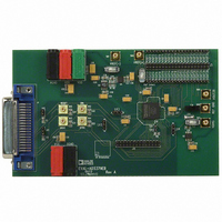
EVAL-AD5379EBZ
Manufacturer Part Number
EVAL-AD5379EBZ
Description
BOARD EVALUATION FOR AD5379
Manufacturer
Analog Devices Inc
Datasheet
1.AD5379ABCZ.pdf
(28 pages)
Specifications of EVAL-AD5379EBZ
Number Of Dac's
40
Number Of Bits
14
Outputs And Type
40, Single Ended
Sampling Rate (per Second)
50k
Data Interface
Serial, Parallel
Settling Time
20µs
Dac Type
Voltage
Voltage Supply Source
Analog and Digital, Dual ±
Operating Temperature
-40°C ~ 85°C
Utilized Ic / Part
AD5379
Lead Free Status / RoHS Status
Lead free / RoHS Compliant


TERMINOLOGY
Relative Accuracy
Relative accuracy, or endpoint linearity, is a measure of the
maximum deviation from a straight line passing through the
endpoints of the DAC transfer function. It is measured after
adjusting for zero-scale error and full-scale error and is
expressed in least significant bits (LSB).
Differential Nonlinearity
Differential nonlinearity is the difference between the measured
change and the ideal 1 LSB change between any two adjacent
codes. A specified differential nonlinearity of 1 LSB maximum
ensures monotonicity.
Zero-Scale Error
Zero-scale error is the error in the DAC output voltage when all
0s are loaded into the DAC register.
Ideally, with all 0s loaded to the DAC and m is all 1s,
c is 10 0000 0000 0000:
Zero-scale error is a measure of the difference between VOUT
(actual) and VOUT (ideal) expressed in mV. Zero-scale error is
mainly due to offsets in the output amplifier.
Full-Scale Error
Full-scale error is the error in DAC output voltage when all 1s
are loaded into the DAC register.
Ideally, with all 1s loaded to the DAC and m is all 1s,
c is 10 0000 0000 0000:
Full-scale error is a measure of the difference between VOUT
(actual) and VOUT (ideal) expressed in mV. It does not include
zero-scale error.
Gain Error
Gain error is the difference between full-scale error and zero-
scale error. It is expressed in mV.
VOUT Temperature Coefficient
This includes output error contributions from linearity, offset,
and gain drift.
DC Output Impedance
DC output impedance is the effective output source resistance.
It is dominated by package lead resistance.
VOUT
VOUT
(VREF(−)− AGND) + REFGND
Gain Error = Full-Scale Error − Zero-Scale Error
(zero scale)
(full scale)
= 3.5 × (VREF(+) − AGND) + 2.5 ×
= 2.5 × (VREF(−) − AGND) + REFGND
Rev. B | Page 15 of 28
DC Crosstalk
The 40 DAC outputs are buffered by op amps that share
common V
changes in one channel (due to an update), this can result in a
further dc change in one or more channel outputs. This effect is
more significant at high load currents and reduces as the load
currents are reduced. With high impedance loads, the effect is
virtually unmeasurable. Multiple V
provided to minimize dc crosstalk.
Output Voltage Settling Time
The amount of time it takes for the output of a DAC to settle to
a specified level for a full-scale input change.
Digital-to-Analog Glitch Energy
The amount of energy injected into the analog output at the
major code transition. It is specified as the area of the glitch in
nV-s. It is measured by toggling the DAC register data between
0x1FFF and 0x2000.
Channel-to-Channel Isolation
Channel-to-channel isolation refers to the proportion of input
signal from one DAC’s reference input that appears at the
output of another DAC operating from another reference. It is
expressed in dB and measured at midscale.
DAC-to-DAC Crosstalk
DAC-to-DAC crosstalk is the glitch impulse that appears at the
output of one converter due to both the digital change and
subsequent analog output change at another converter. It is
specified in nV-s.
Digital Crosstalk
The glitch impulse transferred to the output of one converter
due to a change in the DAC register code of another converter is
defined as the digital crosstalk and is specified in nV-s.
Digital Feedthrough
When the device is not selected, high frequency logic activity
on the device’s digital inputs can be capacitively coupled both
across and through the device to show up as noise on the
VOUT pins. It can also be coupled along the supply and ground
lines. This noise is digital feedthrough.
Output Noise Spectral Density
Output noise spectral density is a measure of internally
generated random noise. Random noise is characterized as a
spectral density (voltage per √Hz). It is measured by loading all
DACs to midscale and measuring noise at the output. It is
measured in nV/(Hz)
DD
and V
SS
1/2
power supplies. If the dc load current
.
DD
and V
SS
terminals are
AD5379
Related parts for EVAL-AD5379EBZ
Image
Part Number
Description
Manufacturer
Datasheet
Request
R


Part Number:
Description:
BOARD EVAL FOR SI270X-A
Manufacturer:
Silicon Laboratories Inc
Datasheet:

Part Number:
Description:
BUCK CONV REF DESIGN KIT IP1201
Manufacturer:
International Rectifier
Datasheet:
Part Number:
Description:
BOARD DEMO SYNC DUAL BUCK CNVTER
Manufacturer:
International Rectifier
Datasheet:
Part Number:
Description:
BOARD DEMO SYNC BUCK CONVETER
Manufacturer:
International Rectifier
Datasheet:

Part Number:
Description:
EVALBOARD/EB Omnidirectional microphone - Analog
Manufacturer:
Analog Devices
Datasheet:
Part Number:
Description:
EVALBOARD/EB Omnidirectional microphone - Analog
Manufacturer:
Analog Devices
Datasheet:


Part Number:
Description:
BOARD EVAL LED DRIVER LT3756
Manufacturer:
Linear Technology
Datasheet:

Part Number:
Description:
BOARD EVAL FOR AD7741/7742
Manufacturer:
Analog Devices Inc
Datasheet:

Part Number:
Description:
±1.7g Dual-Axis IMEMS Accelerometer Evaluation Board
Manufacturer:
Analog Devices Inc
Datasheet:

Part Number:
Description:
IC MULTIPLIER ANALOG 8-SOIC T/R
Manufacturer:
Analog Devices Inc
Datasheet:

Part Number:
Description:
IC ANALOG MULTIPLIER 8-DIP
Manufacturer:
Analog Devices Inc
Datasheet:
Part Number:
Description:
IC ANALOG MULTIPLIER 8-SOIC
Manufacturer:
Analog Devices Inc
Datasheet:
Part Number:
Description:
IC ANALOG MULTIPLIER 8-DIP
Manufacturer:
Analog Devices Inc
Datasheet: