RDK-138 Power Integrations, RDK-138 Datasheet - Page 9
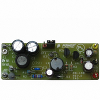
RDK-138
Manufacturer Part Number
RDK-138
Description
KIT REF DESIGN 1.2W PS TN FAMILY
Manufacturer
Power Integrations
Specifications of RDK-138
Mfg Application Notes
LinkSwitch-TN Design Guide, AN-37
Main Purpose
AC/DC, Non-Isolated
Outputs And Type
2, Non-Isolated
Power - Output
1.2W
Voltage - Output
12V, 5V
Current - Output
80mA, 50mA
Voltage - Input
85 ~ 265VAC
Regulator Topology
Buck
Frequency - Switching
66kHz
Board Type
Fully Populated
Utilized Ic / Part
LNK304
Product
Accessories & Kits
Lead Free Status / RoHS Status
Not applicable / Not applicable
Other names
596-1197


DRAIN Voltage .................................. ................ -0.3 V to 700 V
Peak DRAIN Current (LNK302).................200 mA (375 mA)
Peak DRAIN Current (LNK304).................400 mA (750 mA)
Peak DRAIN Current (LNK305).................800 mA (1500 mA)
Peak DRAIN Current (LNK306).................1400 mA (2600 mA)
FEEDBACK Voltage .........................................-0.3 V to 9 V
FEEDBACK Current.............................................100 mA
BYPASS Voltage ..........................................-0.3 V to 9 V
Storage Temperature .......................................... -65 °C to 150 °C
Operating Junction Temperature
Lead Temperature
Thermal Impedance: P or G Package:
Output
Frequency
Maximum Duty
Cycle
FEEDBACK Pin
Turnoff Threshold
Current
FEEDBACK Pin
Voltage at Turnoff
Threshold
DRAIN Supply
Current
CONTROL FUNCTIONS
Parameter
(θ
(θ
(θ
(θ
(4)
JA
JC
JA
JC
........................................................260 °C
) ........................... 70 °C/W
)
) ..................... .... 100 °C/W
)
(1)
D Package:
(2)
............................................... 11 °C/W
............................................... 30 °C/W
Symbol
DC
f
(3)
V
OSC
I
I
I
FB
S1
S2
FB
MAX
..................... -40 °C to 150 °C
ABSOLUTE MAXIMUM RATINGS
SOURCE = 0 V; T
See Notes A, B
FEEDBACK
Switching)
(MOSFET
(Unless Otherwise Specifi ed)
T
J
THERMAL IMPEDANCE
(MOSFET Not Switching)
Open
= 25 °C
(3)
(3)
; 60 °C/W
; 80 °C/W
Conditions
See Figure 7
See Note A
T
S2 Open
V
J
FB
= 25 °C
(4)
(2)
(2)
(2)
(2)
(4)
≥2 V
J
Peak-Peak Jitter
= -40 to 125 °C
Notes:
1. All voltages referenced to SOURCE, T
2. The higher peak DRAIN current is allowed if the DRAIN
3. Normally limited by internal circuitry.
4. 1/16 in. from case for 5 seconds.
5. Maximum ratings specifi ed may be applied, one at a time,
Notes:
1. Measured on pin 2 (SOURCE) close to plastic interface.
2. Measured on pin 8 (SOURCE) close to plastic interface.
3. Soldered to 0.36 sq. in. (232 mm
4. Soldered to 1 sq. in. (645 mm
LNK302/304
Average
to SOURCE voltage does not exceed 400 V.
without causing permanent damage to the product.
Exposure to Absolute Maximum Rating conditions for
extended periods of time may affect product reliability.
LNK305
LNK306
(1,5)
Min
1.54
62
66
30
2
LNK302/304-306
), 2 oz. (610 g/m
Typ
1.65
160
200
220
250
2
66
69
49
), 2 oz. (610 g/m
4
A
Max
= 25 °C.
1.76
220
260
280
310
70
72
68
2
2
) copper clad.
) copper clad.
Units
kHz
μA
μA
μA
%
Rev. I 11/08
V
2-9
9
Related parts for RDK-138
Image
Part Number
Description
Manufacturer
Datasheet
Request
R

Part Number:
Description:
KIT REF DESIGN FOR LNK457D
Manufacturer:
Power Integrations
Datasheet:

Part Number:
Description:
REFERENCE DESIGN LINKSWITCH-PH
Manufacturer:
Power Integrations
Datasheet:

Part Number:
Description:
KIT REF DESIGN FOR LNK403EG
Manufacturer:
Power Integrations
Datasheet:

Part Number:
Description:
KIT REF DESIGN FOR LNK406EG
Manufacturer:
Power Integrations
Datasheet:

Part Number:
Description:
KIT REF DESIGN LINKSWITCH-CV
Manufacturer:
Power Integrations
Datasheet:

Part Number:
Description:
KIT REF DESIGN LINKSWITCH 2
Manufacturer:
Power Integrations
Datasheet:

Part Number:
Description:
Specifications: Family: Eval Boards - DC/DC & AC/DC (Off-Line) SMPS ; Series: HiperLCS™ ; Main Purpose: DC/DC, Step Down ; Outputs and Type: 1, Isolated ; Power - Output: 150W ; Voltage - Output: 24V ; Current - Output: 6.25A ; Voltage - Input:
Manufacturer:
Power Integrations, Inc.
Datasheet:

Part Number:
Description:
KIT DESIGN REF TINYSWITCH-III
Manufacturer:
Power Integrations
Datasheet:

Part Number:
Description:
KIT DESIGN REF LINKSWITCH LP
Manufacturer:
Power Integrations
Datasheet:

Part Number:
Description:
KIT REF DESIGN LED LINKSWITCH TN
Manufacturer:
Power Integrations
Datasheet:
Part Number:
Description:
KIT REF DESIGN PG LINKSWITCH-II
Manufacturer:
Power Integrations
Datasheet:
Part Number:
Description:
REFERENCE DESIGN LINKSWITCH-PL
Manufacturer:
Power Integrations
Datasheet:
Part Number:
Description:
REFERENCE DESIGN LINKSWITCH-PH
Manufacturer:
Power Integrations
Datasheet:

Part Number:
Description:
KIT REF DESIGN 36-72W MOTOR DRVR
Manufacturer:
Power Integrations
Datasheet:
Part Number:
Description:
Specifications: Manufacturer: Power Integrations ; Output Voltage: 380 VDC ; Input / Supply Voltage (Max): 264 VAC ; Input / Supply Voltage (Min): 90 VAC ; Mounting Style: Through Hole ; Output Current: 0.913 A ; Output Power: 347 W
Manufacturer:
Power Integrations, Inc.