RDK-138 Power Integrations, RDK-138 Datasheet - Page 12
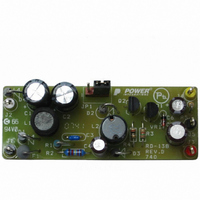
RDK-138
Manufacturer Part Number
RDK-138
Description
KIT REF DESIGN 1.2W PS TN FAMILY
Manufacturer
Power Integrations
Specifications of RDK-138
Mfg Application Notes
LinkSwitch-TN Design Guide, AN-37
Main Purpose
AC/DC, Non-Isolated
Outputs And Type
2, Non-Isolated
Power - Output
1.2W
Voltage - Output
12V, 5V
Current - Output
80mA, 50mA
Voltage - Input
85 ~ 265VAC
Regulator Topology
Buck
Frequency - Switching
66kHz
Board Type
Fully Populated
Utilized Ic / Part
LNK304
Product
Accessories & Kits
Lead Free Status / RoHS Status
Not applicable / Not applicable
Other names
596-1197


Rev. I 11/08
NOTES:
A. Total current consumption is the sum of I
B Since the output MOSFET is switching, it is diffi cult to isolate the switching current from the supply current at the
C. See Typical Performance Characteristics section Figure 14 for BYPASS pin start-up charging waveform.
D. This current is only intended to supply an optional optocoupler connected between the BYPASS and FEEDBACK
E. For current limit at other di/dt values, refer to Figure 13.
F. This parameter is guaranteed by design.
G. This parameter is derived from characterization.
H. Auto-restart on time has the same temperature characteristics as the oscillator (inversely proportional to
Figure 7. LinkSwitch-TN General Test Circuit.
Figure 8. LinkSwitch-TN Duty Cycle Measurement.
2-12
12
switching) and the sum of I
DRAIN. An alternative is to measure the BYPASS pin current at 6 V.
frequency).
pins and not any other external circuitry.
LNK302/304-306
50 V
S2
S1
and I
DSS
when FEEDBACK pin is shorted to SOURCE (MOSFET switching).
470 Ω
5 W
S1
and I
DSS
when FEEDBACK pin voltage is ≥2 V (MOSFET not
S
S
D
FB
BP
S
S
Figure 9. LinkSwitch-TN Output Enable Timing.
(internal signal)
DC
V
DRAIN
t
P
MAX
=
FB
f
OSC
1
470 kΩ
0.1 μF
t P
t EN
S2
50 V
PI-3707-112503
PI-3490-060204
Related parts for RDK-138
Image
Part Number
Description
Manufacturer
Datasheet
Request
R

Part Number:
Description:
KIT REF DESIGN FOR LNK457D
Manufacturer:
Power Integrations
Datasheet:

Part Number:
Description:
REFERENCE DESIGN LINKSWITCH-PH
Manufacturer:
Power Integrations
Datasheet:

Part Number:
Description:
KIT REF DESIGN FOR LNK403EG
Manufacturer:
Power Integrations
Datasheet:

Part Number:
Description:
KIT REF DESIGN FOR LNK406EG
Manufacturer:
Power Integrations
Datasheet:

Part Number:
Description:
KIT REF DESIGN LINKSWITCH-CV
Manufacturer:
Power Integrations
Datasheet:

Part Number:
Description:
KIT REF DESIGN LINKSWITCH 2
Manufacturer:
Power Integrations
Datasheet:

Part Number:
Description:
Specifications: Family: Eval Boards - DC/DC & AC/DC (Off-Line) SMPS ; Series: HiperLCS™ ; Main Purpose: DC/DC, Step Down ; Outputs and Type: 1, Isolated ; Power - Output: 150W ; Voltage - Output: 24V ; Current - Output: 6.25A ; Voltage - Input:
Manufacturer:
Power Integrations, Inc.
Datasheet:

Part Number:
Description:
KIT DESIGN REF TINYSWITCH-III
Manufacturer:
Power Integrations
Datasheet:

Part Number:
Description:
KIT DESIGN REF LINKSWITCH LP
Manufacturer:
Power Integrations
Datasheet:

Part Number:
Description:
KIT REF DESIGN LED LINKSWITCH TN
Manufacturer:
Power Integrations
Datasheet:
Part Number:
Description:
KIT REF DESIGN PG LINKSWITCH-II
Manufacturer:
Power Integrations
Datasheet:
Part Number:
Description:
REFERENCE DESIGN LINKSWITCH-PL
Manufacturer:
Power Integrations
Datasheet:
Part Number:
Description:
REFERENCE DESIGN LINKSWITCH-PH
Manufacturer:
Power Integrations
Datasheet:

Part Number:
Description:
KIT REF DESIGN 36-72W MOTOR DRVR
Manufacturer:
Power Integrations
Datasheet:
Part Number:
Description:
Specifications: Manufacturer: Power Integrations ; Output Voltage: 380 VDC ; Input / Supply Voltage (Max): 264 VAC ; Input / Supply Voltage (Min): 90 VAC ; Mounting Style: Through Hole ; Output Current: 0.913 A ; Output Power: 347 W
Manufacturer:
Power Integrations, Inc.