DM300023 Microchip Technology, DM300023 Datasheet - Page 85
DM300023
Manufacturer Part Number
DM300023
Description
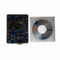
KIT DEMO DSPICDEM SMPS BUCK
Manufacturer
Microchip Technology
Series
dsPIC™r
Datasheets
1.AC164335.pdf
(286 pages)
2.DM300023.pdf
(22 pages)
3.DM300023.pdf
(18 pages)
4.DM300023.pdf
(50 pages)
5.DM300023.pdf
(16 pages)
Specifications of DM300023
Main Purpose
DC/DC, Step Down
Outputs And Type
2, Non-Isolated
Voltage - Input
7 ~ 15V
Regulator Topology
Buck
Board Type
Fully Populated
Utilized Ic / Part
dsPIC30F2020
Processor To Be Evaluated
dsPIC30F202x/1010
Interface Type
RS-232
Lead Free Status / RoHS Status
Lead free / RoHS Compliant
Current - Output
-
Voltage - Output
-
Power - Output
-
Frequency - Switching
-
Lead Free Status / Rohs Status
Lead free / RoHS Compliant
Available stocks
Company
Part Number
Manufacturer
Quantity
Price
Company:

Part Number:
DM300023
Manufacturer:
Microchip Technology
Quantity:
135
Company:
Part Number:
DM300023
Manufacturer:
MICROCHIP
Quantity:
12 000


7.6
A complete programming sequence is necessary for
programming or erasing the internal Flash in RTSP
mode. A programming operation is nominally 2 msec in
duration and the processor stalls (waits) until the oper-
ation is finished. Setting the WR bit (NVMCON<15>)
starts the operation, and the WR bit is automatically
cleared when the operation is finished.
7.6.1
The user can erase and program one row of program
Flash memory at a time. The general process is:
1.
2.
3.
EXAMPLE 7-1:
© 2006 Microchip Technology Inc.
; Setup NVMCON for erase operation, multi word write
; program memory selected, and writes enabled
; Init pointer to row to be ERASED
Read one row of program Flash (32 instruction
words) and store into data RAM as a data
“image”.
Update the data image with the desired new
data.
Erase program Flash row.
a)
b)
c)
d)
e)
f)
g)
Programming Operations
Setup NVMCON register for multi-word,
program Flash, erase and set WREN bit.
Write address of row to be erased into
NVMADRU/NVMDR.
Write ‘55’ to NVMKEY.
Write ‘AA’ to NVMKEY.
Set the WR bit. This will begin erase cycle.
CPU will stall for the duration of the erase
cycle.
The WR bit is cleared when erase cycle
ends.
MOV
MOV
MOV
MOV
MOV
MOV
DISI
MOV
MOV
MOV
MOV
BSET
NOP
NOP
PROGRAMMING ALGORITHM FOR
PROGRAM FLASH
#0x4041,W0
W0
#tblpage(PROG_ADDR),W0
W0
#tbloffset(PROG_ADDR),W0
W0, NVMADR
#5
#0x55,W0
W0
#0xAA,W1
W1
NVMCON,#WR
,
,
,
,
ERASING A ROW OF PROGRAM MEMORY
NVMCON
NVMADRU
NVMKEY
NVMKEY
Preliminary
;
; Init NVMCON SFR
;
; Initialize PM Page Boundary SFR
; Intialize in-page EA<15:0> pointer
; Intialize NVMADR SFR
; Block all interrupts with priority <7
; for next 5 instructions
; Write the 0x55 key
;
; Write the 0xAA key
; Start the erase sequence
; Insert two NOPs after the erase
; command is asserted
4.
5.
6.
7.6.2
Example 7-1 shows a code sequence that can be used
to erase a row (32 instructions) of program memory.
dsPIC30F1010/202X
Write 32 instruction words of data from data
RAM “image” into the program Flash write
latches.
Program 32 instruction words into program
Flash.
a)
b)
c)
d)
e)
f)
Repeat steps 1 through 5 as needed to program
desired amount of program Flash memory.
Setup NVMCON register for multi-word,
program Flash, program and set WREN bit.
Write ‘55’ to NVMKEY.
Write ‘AA’ to NVMKEY.
Set the WR bit. This will begin program
cycle.
CPU will stall for duration of the program
cycle.
The WR bit is cleared by the hardware
when program cycle ends.
ERASING A ROW OF PROGRAM
MEMORY
DS70178C-page 83
Related parts for DM300023
Image
Part Number
Description
Manufacturer
Datasheet
Request
R

Part Number:
Description:
Manufacturer:
Microchip Technology Inc.
Datasheet:
Part Number:
Description:
Manufacturer:
Microchip Technology Inc.
Datasheet:
Part Number:
Description:
Manufacturer:
Microchip Technology Inc.
Datasheet:
Part Number:
Description:
Manufacturer:
Microchip Technology Inc.
Datasheet:
Part Number:
Description:
Manufacturer:
Microchip Technology Inc.
Datasheet:
Part Number:
Description:
Manufacturer:
Microchip Technology Inc.
Datasheet:
Part Number:
Description:
Manufacturer:
Microchip Technology Inc.
Datasheet:
Part Number:
Description:
Manufacturer:
Microchip Technology Inc.
Datasheet: