CRD4525-Q1 Cirrus Logic Inc, CRD4525-Q1 Datasheet
CRD4525-Q1
Specifications of CRD4525-Q1


Related parts for CRD4525-Q1


CRD4525-Q1 Summary of contents
Page 1
W Digital Audio Amplifier with Integrated ADC Digital Amplifier Features Fully Integrated Power MOSFETs No Heatsink Required – Programmable Power Foldback on Thermal Warning – High Efficiency > 100 dB Dynamic Range < 0.1% THD Configurable ...
Page 2
... The CS4525 is available in a 48-pin QFN package in Commercial grade (0° to +70° C). The CRD4525-Q1 4- layer, 1 oz. copper and CRD4525-D1 2-layer, 1 oz. cop- per customer reference designs are also available. ...
Page 3
TABLE OF CONTENTS 1. PIN DESCRIPTIONS - SOFTWARE MODE .......................................................................................... 8 2. PIN DESCRIPTIONS - HARDWARE MODE ....................................................................................... 10 2.1 Digital I/O Pin Characteristics ........................................................................................................ 12 3. TYPICAL CONNECTION DIAGRAMS ................................................................................................. 13 4. TYPICAL SYSTEM CONFIGURATION DIAGRAMS ........................................................................... 15 5. ...
Page 4
Power-Down Sequence ............................................................................................ 55 6.2.3 Input Source Selection .......................................................................................................... 55 6.2.4 PWM Channel Delay ............................................................................................................ 55 6.2.5 Digital Signal Flow ................................................................................................................ 56 6.2.5.1 High-Pass Filter ........................................................................................................ 56 6.2.5.2 Mute Control ............................................................................................................. 56 6.2.5.3 Warning and Error Reporting .................................................................................... 56 ...
Page 5
Enable Foldback Floor (EnFloor) .......................................................................................... 75 9.5.6 Ramp Speed (RmpSpd[1:0]) ................................................................................................ 75 9.6 Mixer / Pre-Scale Configuration (Address 06h) ............................................................................. 75 9.6.1 Pre-Scale Attenuation (PreScale[2:0]) .................................................................................. 75 9.6.2 Right Channel Mixer (RChMix[1:0]) ...................................................................................... 76 9.6.3 Left Channel Mixer (LChMix[1:0]) ...
Page 6
Power Control (Address 5Fh) ...................................................................................................... 88 9.19.1 Automatic Power Stage Retry (AutoRetry) ......................................................................... 88 9.19.2 Enable Over-Current Protection (EnOCProt) ...................................................................... 88 9.19.3 Select VD Level (SelectVD) ................................................................................................ 88 9.19.4 Power Down ADC (PDnADC) ............................................................................................. 88 9.19.5 Power Down PWM ...
Page 7
Figure 16.Bi-Quad Filter Architecture ........................................................................................................ 33 Figure 17.Peak Signal Detection & Limiting .............................................................................................. 37 Figure 18.Foldback Process ..................................................................................................................... 40 Figure 19.Popguard Connection Diagram ................................................................................................. 46 Figure 20.2-Channel Full-Bridge PWM Output Delay ............................................................................... 50 Figure 21.3-Channel PWM Output Delay .................................................................................................. 50 ...
Page 8
PIN DESCRIPTIONS - SOFTWARE MODE 48 INT 1 SCL 2 SDA 3 LRCK 4 SCLK 5 SDIN 6 HP_DETECT/MUTE 7 RST 8 LVD 9 DGND 10 VD_REG Pin Name Pin # INT 1 Interrupt (Output) ...
Page 9
VD Voltage Level Indicator (Input) - Identifies the voltage level attached to VD. When applying LVD 9 5 VD, LVD must be connected to VD. When applying 2 3 VD, LVD must be DGND. ...
Page 10
PIN DESCRIPTIONS - HARDWARE MODE 48 CLK_FREQ0 1 CLK_FREQ1 2 ADC/SP 3 LRCK 4 SCLK 5 SDIN 6 MUTE 7 RST 8 LVD 9 DGND 10 VD_REG Pin Name Pin # CLK_FREQ0 1 Clock Frequency ...
Page 11
VD Voltage Level Indicator (Input) - Identifies the voltage level attached to VD. When applying LVD 9 5 VD, LVD must be connected to VD. When applying 2 3 VD, LVD must be con- ...
Page 12
Digital I/O Pin Characteristics The logic level for each input is set by its corresponding power supply and should not exceed the maximum ratings. Power Pin Pin Name Supply Number Software Mode VD 1 INT 2 SCL 3 SDA ...
Page 13
TYPICAL CONNECTION DIAGRAMS +3 µF Analog Audio Inputs Analog Audio Switch Analog Monitor Output Crystal 24.576 MHz MPEG Audio Processor - or - HDMI Receiver Lip-Synch Delay NJU26902 +2.5V 0.1 µF 10 µF VD Micro- ...
Page 14
V 10 µF Analog Audio Inputs Analog Audio Switch Analog Monitor Output Audio Processor Clock 24.576 MHz VD Micro- Controller 10 µF 0.1 µF Figure 2. Typical Connection Diagram - Hardware Mode 14 0.1 µF 470 µF ...
Page 15
TYPICAL SYSTEM CONFIGURATION DIAGRAMS Main Tuner PIP Tuner A A/V Switch A A Main Tuner PIP Tuner A A/V Switch A A DS726PP3 ...
Page 16
Main Tuner PIP Tuner A A/V Switch A A Stereo + Subwoofer Analog Out Sound Processor Analog In Control Port Audio Delay 18.432 MHz Crystal ...
Page 17
Main Tuner PIP Tuner A A/V Switch A A DS726PP3 Bi-Amp Stereo with Subwoofer Output Analog Out Sound Processor Analog Digital In Out Control Port Audio Delay 18.432 MHz Crystal ...
Page 18
CHARACTERISTICS AND SPECIFICATIONS RECOMMENDED OPERATING CONDITIONS AGND = DGND = PGND = 0 V; all voltages with respect to ground. Parameters DC Power Supply Digital and Analog Core Amplifier Outputs Temperature Ambient Temperature Junction Temperature Notes: 1. For VD ...
Page 19
ANALOG INPUT CHARACTERISTICS Test Conditions (unless otherwise specified): AGND = DGND = PGND = 0 V; All voltages with respect to ground 25° 3.3 V; Input Signal: 1 kHz sine wave through the recommended passive input ...
Page 20
PWM POWER OUTPUT CHARACTERISTICS Test Conditions (unless otherwise specified): AGND = DGND = PGND = 0 V; All voltages with respect to ground 25° 3 OutputDly[3:0] = 1111; PhaseShift ...
Page 21
SERIAL AUDIO INPUT PORT SWITCHING SPECIFICATIONS AGND = DGND = PGND = Parameters Supported Input Sample Rates LRCK Duty Cycle SCLK Frequency SCLK Duty Cycle LRCK Setup Time Before SCLK Rising Edge SDIN Setup Time Before ...
Page 22
AUX SERIAL AUDIO I/O PORT SWITCHING SPECIFICATIONS AGND = DGND = PGND = Logic 0 = DGND; Logic 1 = VD; (Note 11) Parameters Input Source: Analog Inputs (Internal ADC) Output Sample Rate (Note 16) AUX_LRCK Duty ...
Page 23
XTI SWITCHING SPECIFICATIONS Parameter External Crystal Operating Frequency (Notes 15, 16) XTI Duty Cycle Notes: 15. External crystal oscillator mode only available in Software Mode. SYS_CLK SWITCHING SPECIFICATIONS AGND = DGND = PGND = ...
Page 24
I²C CONTROL PORT SWITCHING SPECIFICATIONS AGND = DGND = PGND = Parameter SCL Clock Frequency RST Rising Edge to Start Bus Free Time Between Transmissions Start Condition Hold Time (prior to first clock pulse) Clock Low ...
Page 25
DC ELECTRICAL CHARACTERISTICS AGND = DGND = PGND = 0 V; All voltages with respect to ground; PWM switch rate = 384 kHz; Unless otherwise specified. Parameters Normal Operation (Note 18) Power Supply Current Power Dissipation Power-Down Mode (Note 19) ...
Page 26
APPLICATIONS 6.1 Software Mode Maximum device flexibility and features are available when the CS4525 is used in software mode. The avail- able features are described in the following sections. All device configuration is achieved via the I²C control port ...
Page 27
Crystal Oscillator Mode To use an external crystal in conjunction with the internal crystal driver fundamental mode par- allel resonant crystal must be connected between the XTI and XTO pins. This crystal must oscillate within the ...
Page 28
Power-Up and Power-Down The CS4525 will remain in a completely powered-down state with the control port inaccessible until the RST pin is brought high. Once RST is high, the control port will be accessible, but all other internal blocks ...
Page 29
Input Source Selection The CS4525 can accept analog or digital audio input signals. Digital audio input signals are supplied through the serial audio input port as outlined in signals are supplied through the internal ADC as outlined in is ...
Page 30
Pre-Scaler Applying any gain to a full-scale signal in the digital domain will cause the signal to clip. To prevent this, a pre-scaler block is included prior to the internal digital signal processing blocks. This allows the input signal ...
Page 31
De-Emphasis The CS4525 includes an on-chip digital de-emphasis filter optimized for a sample rate of 44.1 kHz to ac- commodate audio recordings that utilize 50/15 µs pre-emphasis equalization as a means of noise reduc- tion. The filter response is ...
Page 32
Input Sample Rate 32 kHz 44.1 kHz 48 kHz, 96 kHz The cut/boost level of the bass and treble shelving filters are set by the Bass[3:0] and Treble[3:0] bits in the Tone Control register. Referenced Control Register Location EnToneCtrl .......................... ...
Page 33
Parametric EQ The CS4525 implements 5 fully programmable parametric EQ filters. The filters are implemented in the bi-quad form shown below. x[n] This architecture is represented by the equation shown below where y[n] represents the output sample value and ...
Page 34
Adaptive Loudness Compensation The CS4525 includes adaptive loudness compensation to enhance the audibility of program material at low volume levels. The adaptive loudness compensation feature operates by varying the bass and treble boost of the tone control shelving filters ...
Page 35
Bass Management The CS4525 implements a dedicated stereo 24 dB/octave Linkwitz-Riley crossover with adjustable cross- over frequency to achieve bass management for 2.1 configurations. The filter’s stereo high-pass outputs are used to drive the full-range speakers, and its stereo ...
Page 36
Volume and Muting Control The CS4525’s volume control architecture provides the ability to control the level of each output channel on both an individual and master basis. Individual control allows the volume and mute state of a single channel ...
Page 37
Peak Signal Limiter When enabled, the limiter monitors the digital output following the volume control block, detects when peak levels exceed a selectable maximum threshold level and lowers the volume at a programmable at- tack rate until the signal ...
Page 38
When the LimitAll feature is activated, attenuation will be applied to all channels when a single channel exceeds the maximum threshold and released when the level of all channels is below the minimum threshold. When the LimitAll feature is de-activated, ...
Page 39
Thermal Limiter The CS4525 implements a thermal limiter function to provide a quick corrective response to potentially damaging thermal overload conditions. The thermal limiter feature operates by sensing the presence of a thermal warning condition and, in response, utilizes ...
Page 40
Thermal Foldback The CS4525 implements comprehensive thermal foldback features to guard against damaging thermal overload conditions. Thermal foldback is similar to the thermal limiting described on features attenuate the output signal in response to thermal warnings conditions; however, thermal ...
Page 41
The AttackDly[1:0] bits in the Foldback Cfg register allow the foldback attack delay timeout period to be adjusted from approximately 0.5 seconds to approximately 2.0 seconds. The maximum attenuation ap- plied by the thermal foldback algorithm can be restricted to ...
Page 42
Crossover & Sensitivity Control The CS4525 implements a dedicated stereo 24 dB/octave Linkwitz-Riley crossover filter with adjustable cross-over frequency and sensitivity control to facilitate 2-way speaker configurations. The filter’s high- pass output can be used to drive the ...
Page 43
Auxiliary Serial Output The CS4525 includes a stereo auxiliary serial output which allows an external device to leverage on its internal signal processing and routing capabilities. The auxiliary serial output can receive its data from any of the sources ...
Page 44
Serial Audio Delay & Warning Input Port The CS4525 includes a configurable delay and warning port to allow easy system integration of external lip-sync delay devices or warning inputs from external amplifiers. The port can be configured as a ...
Page 45
Powered PWM Outputs The CS4525’s 3 internal modulators can be used to generate multiple powered PWM output configura- tions to enable a wide variety of system implementations. The CS4525 also implements PWM Popguard to minimize output transients in half-bridge ...
Page 46
The Popguard technology has no effect on the PWM_SIG outputs nor the aux- iliary serial output. +8V to +18V The PWM Popguard feature is disabled by default; to enable it, the RmpSpd[1:0] register must be set to ...
Page 47
Recommended PWM_SIG Power-Up Sequence for an External PWM Amplifier 1. Engage the reset/power-down feature of the external PWM amplifier. 2. Set the PDnAll bit in the Power Ctrl register to stop the PWM modulators not already ...
Page 48
Recommended PWM_SIG Power-Up Sequence for Headphone & Line- Out 1. Set the PDnAll bit in the Power Ctrl register to stop the PWM modulators not already set. 2. Configure the PWM_SIG outputs as desired via the ...
Page 49
PWM_SIG Logic-Level Output Configurations Four channel mapping output configurations are supported for the PWM_SIG output pins as shown in Table 10 below. The configurations support stereo, channel 1 with sub, and channel 2 with sub applica- tions. When disabled, ...
Page 50
PWM Modulator Configuration The CS4525 PWM modulators support flexible configuration options designed to simplify system integra- tion. Delays may be inserted between the switching edges on adjacent channels to manage noise, and the PWM switching frequency can be easily ...
Page 51
PWM AM Frequency Shift When using a PWM amplifier in a system containing an AM tuner possible that the PWM switch rate conflicts with the desired tuning frequency of the AM tuner. To overcome this effect, the ...
Page 52
HiZPSig HP/Mute HP_DETECT Setting Setting /MUTE Input Not Active (Mute Mode) 1 Active Not Active 1 (Head- phone Active Mode) *Signals denoted with one asterisk do not have Bass Manager, 2-Way Crossover, or Channel Mix applied. ...
Page 53
Interrupt Reporting The CS4525 has comprehensive interrupt reporting capabilities. Many conditions including SRC lock, ADC overflow, digital data path overflow, and amplifier errors can cause an interrupt. The INT output pin is intended to drive an interrupt input pin ...
Page 54
Hardware Mode A limited feature set is available when the CS4525 powers up in hardware mode. The available features are described in the following sections. All device configuration is achieved via hardware control input pins. 6.2.1 System Clocking In ...
Page 55
Power-Down Sequence 1. Bring MUTE low to mute the device’s outputs and minimize audible pops. 2. Bring RST low to halt the operation of the device. The device’s power consumption will be brought to an absolute minimum. 3. The ...
Page 56
Digital Signal Flow In hardware mode, the CS4525 operates as a 2-channel full-bridge PWM amplifier with analog or digital inputs. Both the PWM outputs and the auxiliary serial outputs are unavailable in hardware mode. To pro- tect against over-temperature ...
Page 57
Thermal Foldback In hardware mode, the CS4525 implements a thermal foldback feature to guard against damaging thermal overload conditions. The thermal foldback feature begins limiting the volume of the digital audio input to the amplifier stage as the junction ...
Page 58
Automatic Power Stage Shut-Down To protect itself from permanent damage, the CS4525 will automatically shut down its internal PWM pow- er output stages when a thermal error, PWM power output over-current error under-voltage condi- tion occurs. In ...
Page 59
Output Filters The output filter configuration of the CS4525 can greatly affect device performance. These components re- duce radiated EMI, protect the output transistors of the device, attenuate the high frequency content of the output signal, and, in the ...
Page 60
Full-Bridge Output Filter (Stereo or Parallel) Figure 27 shows the output filter for stereo full-bridge and parallel full-bridge output configurations. Tran- sient voltage suppression circuits are implemented snubber networks comprised of resistors R (5.6 Ω, 1/8 ...
Page 61
Analog Inputs Very few components are required to interface between the audio source and the CS4525’s analog inputs, AINL and AINR. A single order passive low-pass filter is recommended to prevent high-frequency content from aliasing into the audio band ...
Page 62
Serial Audio Interfaces The CS4525 interfaces to external digital audio devices via the serial audio input port and the auxiliary/delay serial ports. The serial audio input port provides support for I²S, Left-Justified and Right-Justified data formats and op- erates ...
Page 63
Right-Justified Data Format In Right-Justified format, data is received most significant bit first and with the least significant bit present the last SCLK before the LRCK transition and is valid on the rising edge of SCLK. For ...
Page 64
I²C Control Port Description and Timing The control port is used to access the registers allowing the CS4525 to be configured for the desired oper- ational modes and formats. The operation of the control port may be completely asynchronous ...
Page 65
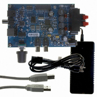
... This pad must mate with an equally dimensioned copper pad on the PCB and must be electrically connected to ground. A series of thermal vias should be used to connect this copper pad to one or more larger ground planes on other PCB layers. The CRD4525 reference design demon- strates the optimum thermal pad and via configuration. ...
Page 66
REGISTER QUICK REFERENCE This table shows the register names and their associated default values. Adr Name 7 01h Clock Config EnSysClk DivSysClk page 69 1 02h Input Config ADC/SP EnAnHPF page 71 0 03h Aux Config EnAuxPort DlyPortCfg1 DlyPortCfg0 ...
Page 67
Adr Name 7 25h MSB ............................................................................................................................. BiQuad 2 26h MSB-8 ............................................................................................................................. B2 Coeff 27h LSB+7 ............................................................................................................................. 28h MSB ............................................................................................................................. BiQuad 3 29h MSB-8 ............................................................................................................................. A1 Coeff 2Ah LSB+7 ............................................................................................................................. 2Bh MSB ............................................................................................................................. BiQuad 3 2Ch MSB-8 ............................................................................................................................. A2 Coeff 2Dh ...
Page 68
Adr Name 7 55h Volume Cfg SZCMode1 SZCMode0 Mute50/50 page 80 1 56h Sensitivity LowPass3 LowPass2 page 81 0 57h Master Vol MVol7 MVol6 page 82 0 58h Ch A Vol ChAVol7 ChAVol6 page 83 0 59h Ch B Vol ...
Page 69
REGISTER DESCRIPTIONS All registers are read/write unless otherwise stated. All “Reserved” bits must maintain their default state. 9.1 Clock Configuration (Address 01h EnSysClk DivSysClk ClkFreq1 9.1.1 SYS_CLK Output Enable (EnSysClk) Default = 1 Function: This bit controls ...
Page 70
HP_Detect/Mute Pin Active Logic Level (HP/MutePol) Default = 0 Function: This bit determines the active logic level for the HP_DETECT/MUTE input signal. HP/MutePol Setting Headphone Detect/Mute Input Polarity 0 .......................................... Active low. 1 .......................................... Active high. 9.1.5 HP_Detect/Mute Pin ...
Page 71
Input Configuration (Address 02h ADC/SP EnAnHPF Reserved 9.2.1 Input Source Selection (ADC/SP) Default = 0 Function: This bit selects the audio input source. ADC/SP Setting Audio Input Source 0 ..........................................Digital input from the serial audio input port. ...
Page 72
AUX Port Configuration (Address 03h EnAuxPort DlyPortCfg1 DlyPortCfg0 9.3.1 Enable Aux Serial Port (EnAuxPort) Default = 0 Function: Controls the operation of the auxiliary serial port. EnAuxPort Setting Auxiliary Port State 0 .......................................... Auxiliary port disabled. 1 ...
Page 73
Aux Serial Port Left Channel Data Select (LChDSel[1:0]) Default = 00 Function: Selects the data to be sent over the left channel of the auxiliary port serial data output signal. LChDSel[1:0] Setting Aux Serial Port Left Channel Output Data ...
Page 74
PDnAll bit is set). Attempts to write these bits while the PDnAll bit is cleared will be ignored. See on page 55 for more information. ...
Page 75
Foldback Attack Delay (AttackDly[1:0]) Default = 01 Function: Controls the foldback attack delay. See AttackDly[1:0] Setting Foldback Attack Time 00 ........................................Approximately 0.5 seconds. 01 ........................................Approximately 1.0 seconds. 10 ........................................Approximately 1.5 seconds. 11.........................................Approximately 2.0 seconds. 9.5.5 Enable Foldback Floor (EnFloor) ...
Page 76
Right Channel Mixer (RChMix[1:0]) Default = 00 Function: Controls the right channel mixer output. See RChMix[1:0] Setting Right Channel Mixer Output on Channel B 00 ........................................ Right Channel 01 ........................................ (Left Channel + Right Channel ........................................ ...
Page 77
Digital Signal Processing High-Pass Filter (EnDigHPF) Default = 0 Function: Controls the operation of the digital signal processing high-pass filter. See High-Pass Filter” on page 30 EnDigHPF Setting Digital Signal Processing High-Pass Filter State 0 ..........................................Digital signal processing high-pass ...
Page 78
Tone Control (Address 08h Treble3 Treble2 Treble1 9.8.1 Treble Gain Level (Treb[3:0]) Default = 1000 Function: Sets the gain/attenuation level of the treble shelving filter.The level can be adjusted in 1.5 dB steps from +12.0 to -10.5 ...
Page 79
Hi-Z PWM_SIG Outputs (HiZPSig) Default = 0 Function: When cleared, the PWM_SIG1 and PWM_SIG2 output drivers are placed in a high-impedance state. When set, the PWM_SIG1 and PWM_SIG2 output drivers are active. It should be noted that the function ...
Page 80
Volume and 2-Way Cross-Over Configuration (Address 55h SZCMode1 SZCMode0 Mute50/50 9.10.1 Soft Ramp and Zero Cross Control (SZCMode[1:0]) Default = 10 Function: Sets the soft ramp and zero crossing detection modes by which volume and muting changes ...
Page 81
Enable 2-Way Crossover (En2Way) Default = 0 Function: Enables the 2-way crossover filters for channel 1 and channel 2. En2Way Setting 2-Way Crossover State 0 ..........................................2-way crossover disabled. 1 ..........................................2-way crossover enabled. 9.10.5 2-Way Cross-Over Frequency (2WayFreq[2:0]) Default = ...
Page 82
Channel A and Channel B High-Pass Sensitivity Adjust (HighPass[3:0]) Default = 0000 Function: Controls the 2-way cross-over high-pass sensitivity adjustment. See trol” on page 42 for more information. HighPass[3:0] Setting Sensitivity Compensation Level 0000 .................................... 0.0 dB 0001 .................................... ...
Page 83
Channel A and B Volume Control (Address 58h & 59h ChXVol7 ChXVol6 ChXVol5 9.13.1 Channel X Volume Control (ChXVol[7:0]) Default = 30h Function: Sets the gain/attenuation levels of channel A and channel B. See page 36 for ...
Page 84
Mute/Invert Control (Address 5Bh InvADC InvSub InvCh2 9.15.1 ADC Invert Signal Polarity (InvADC) Default = 0 Function: When set, the signal polarity of the ADC will be inverted. InvADC Setting ADC Signal Inversion State 0 .......................................... ADC ...
Page 85
See “Volume and Muting Control” on page 36 MuteChX Setting Channel X PWM Mute State 0 ..........................................Channel X PWM outputs un-muted. 1 ..........................................Channel X PWM ...
Page 86
Peak Signal Limit All Channels (LimitAll) Default = 1 Function: When cleared, the peak signal limiter will limit the maximum signal amplitude to prevent clipping on the specific channel indicating clipping. The other channels will not be affected. When ...
Page 87
Limiter Configuration 2 (Address 5Dh Reserved Reserved RRate5 9.17.1 Limiter Release Rate (RRate[5:0]) Default = 111111 Function: Sets the rate at which the limiter releases the digital attenuation from levels below the minimum setting in the limiter ...
Page 88
Power Control (Address 5Fh AutoRetry EnOCProt SelectVD 9.19.1 Automatic Power Stage Retry (AutoRetry) Default = 1 Function: Enables the Auto-Retry function upon over-current error. See page 53. AutoRetry Setting Auto-Retry State 0 .......................................... Auto-Retry feature disabled. 1 ...
Page 89
Power Down PWM Power Output X (PDnOutX) Default = 1 Function: When set, the specific PWM power output will enter a power-down state. Only the output power stage is powered down. The PWM modulator is not affected, nor is ...
Page 90
SRC Lock State Transition Interrupt (SRCLock) Function: This bit is read only. When set, indicates that the SRC has transitioned from an unlock to lock state or from a lock state to an unlock state since the last read ...
Page 91
Amplifier Error Interrupt Bit (AmpErr) Function: This bit is read only. When set, indicates that an error was detected in the power amplifier section since the last read of this register. This interrupt bit is an edge-triggered event and ...
Page 92
Mask for Amplifier Error (AmpErrM) Default = 0 Function: This bit serves as a mask for the amplifier error interrupt sources. If this bit is set, the AmpErr interrupt is unmasked, meaning that if the AmpErr bit is set, ...
Page 93
Channel X Overflow (ChXOvflSt) Function: These bits are read only and will identify the presence of an overflow condition anywhere in the associated channel’s signal path. When set, indicates that an over-range condition is currently occurring in the chan- ...
Page 94
Under Voltage / Thermal Error State (UVTE[1:0]) Function: Indicates the operational status of the amplifier. These bits can identify a Thermal Warning condition, a Thermal Error condition Under Voltage condition. The thresholds for each of these conditions ...
Page 95
DEFINITIONS Dynamic Range (DYR) The ratio of the rms value of the signal to the rms sum of all other spectral components over the specified bandwidth, typically kHz. Dynamic Range is a signal-to-noise ratio measurement ...
Page 96
DIMENSIONS 48L QFN (9 × BODY) PACKAGE DRAWING D Pin #1 ID Top View INCHES DIM MIN 0.0000 b 0.0118 0.0138 D 0.3543 BSC D2 0.2618 0.2677 E 0.3543 BSC E2 0.2618 0.2677 e ...
Page 97
... Board 2 Layer / 1oz. Copper CRD4525-D1 Reference Design Board DS726PP3 Symbol θ RMS-OUT Package Temp Range Container Pb-Free Grade 48-QFN Yes Commercial - - - - - - CS4525 Min Typ Max - 1 - °C/Watt (assuming 85% efficiency) Order# Rail CS4525-CNZ 0° to +70°C Tape and CS4525-CNZR Reel - - CRD4525- CRD4525-D1 Units 97 ...
Page 98
HISTORY Release The following items were updated: “Analog Input Characteristics” on page 19 “PWM Power Output Characteristics” on page 20 “XTI Switching Specifications” on page 23 “SYS_CLK Switching Specifications” on page 23 PP1 “Digital Interface Specifications” on page 25 ...