EVAL-AD7674CB Analog Devices Inc, EVAL-AD7674CB Datasheet - Page 3
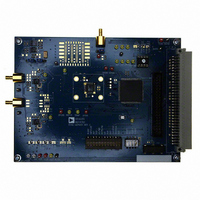
EVAL-AD7674CB
Manufacturer Part Number
EVAL-AD7674CB
Description
BOARD EVAL FOR AD7674
Manufacturer
Analog Devices Inc
Series
PulSAR®r
Specifications of EVAL-AD7674CB
Number Of Adc's
1
Number Of Bits
18
Sampling Rate (per Second)
800k
Data Interface
Serial, Parallel
Inputs Per Adc
1 Differential
Input Range
0 ~ 5 V
Power (typ) @ Conditions
126mW @ 800kSPS
Voltage Supply Source
Analog and Digital
Operating Temperature
-40°C ~ 85°C
Utilized Ic / Part
AD7674
Lead Free Status / RoHS Status
Contains lead / RoHS non-compliant


Preliminary Technical Data
OVERVIEW
Figure 1 shows a block diagram of the EVAL-AD76XXCB
evaluation board. When used in stand-alone mode or in
conjunction with the EVAL-CONTROL BRDX, the gate array,
U10, provides the necessary control signals for conversion and
buffers the ADC data. The evaluation board is a flexible design
that enables the user to choose among many different board
configurations, analog signal conditioning, reference, and
different modes of conversion data.
CONVERSION CONTROL/ MASTER CLOCK
Conversion start ( CNVST ) controls the sample rate of the ADC
and is the only input needed for conversion; all SAR timing is
generated internally. CNVST is generated either by the gate
array or externally via J3 (SMB) and setting JP22 in the external
(EXT) position. The evaluation board is factory configured for
the CNVST range shown in Table 1. Externally generated
CNVST should have very low jitter and sharp edges for the
maximum dynamic performance of the part. Since CNVST
jitter usually results in poor SNR performance, it is
recommended to use the on-board CNVST generation
whenever possible.
The master clock (MCLK) source for the gate array is generated
from the DSP CLKOUT pin (buffered) when using the EVAL-
CONTROL BRDX or form U12, the 40MHz local oscillator
slectabel when using the accompanying software. The range for
CNVST in Table 1 is a ratio generated from this master clock. In
stand-alone mode, other clock frequencies can be used to
change the gate array generated CNVST by this ratio. However,
other timings will be affected – namely the slave serial clock
(SCLK) interface. In serial slave mode, SCLK = MCLK.
While the ADC is converting, activity on the BUSY pin turns on
the LED, D2. Additionally, the BUSY signal can be monitored
test point TP1. Buffered conversion data (BD) is available at
U10 on the output bus BD[0:15] on the 40-pin IDC connector
P2, and on the 96-pin connector P3. When operating with the
EVAL-CONTROL-BRDX, data is transferred using a 16 bit bus
and corresponding word and byte modes selectable with the
software. For the 18 bit converters two consecutive 16 bit words
are read, however, the ADC data is still read into the gate array
as 18 bits. Additionally, BD is updated on the falling edge of
BBUSY on P3-C17, and on the rising edge of DBUSY on P2-33.
When either parallel or serial reading mode of the ADC is used,
data is available on this parallel bus.
When using Serial Mode, serial data is available at T3, T4, T5,
and T6 (SDOUT, SCLK, SYNC and RDERROR) and buffered
serial data is output on TP17, TP18, and TP19 (SCLK, SYNC,
and SDOUT). When using Slave Serial Mode, the external serial
clock SCLK applied to the ADC is the MCLK, U12, frequency
(40MHz). Refer to the device specific datasheet for full details
of the interface modes.
Rev. PrW | Page 3 of 22
Part
AD7610
AD7612
AD7621
AD7622
AD7623
AD7631
AD7634
AD7641
AD7643
AD7650
AD7651
AD7652
AD7653
AD7654
AD7655
AD7660
AD7661
AD7663
AD7664
AD7665
AD7666
AD7667
AD7671
AD7674
AD7675
AD7676
AD7677
AD7678
AD7679
AD7951
Table 1. CNVST Generation, Analog Input Range
ANALOG INPUT
The analog input amplifier circuitry U6 and U7 (see schematic -
Figure 2) allows flexible configuration changes such as positive
or negative gain, input range scaling, filtering, addition of a DC
component, use of different op-amp and supplies depending on
the ADC. The analog input amplifiers are set as unity gain
buffers at the factory. The supplies are selectable with solder
pads JP8 (VDRV+) and JP3 (VDRV-) and are set for the ±12V
range. Table 1 shows the analog input range for the available
evaluation boards.
The default configuration for the single ended (SE) unipolar
ADCs sets U6 at mid-scale from the voltage divider (V
Res
(bits)
16
16
16
16
16
16
16
18
18
16
16
16
16
16
16
16
16
16
16
16
16
16
16
18
16
16
16
18
18
14
Sample
Rate
250kSPS
750kSPS
3MSPS
2MSPS
1.33MSPS
250kSPS
670kSPS
2MSPS
1.25MSPS
571KSPS
100KSPS
500KSPS
1MSPS
500KSPS
500KSPS
100KSPS
100KSPS
250KSPS
571KSPS
571KSPS
500KSPS
1MSPS
1MSPS
800KSPS
100KSPS
500KSPS
1MSPS
100KSPS
571KSPS
1MSPS
Analog Input
Range
0-5V, 0-10V,
+/-5V, +/-10V
0-5V, 0-10V,
+/-5V, +/-10V
0 to 2.5V
0 to 2.5V
0 to 2.5V
0-5V, 0-10V,
+/-5V, +/-10V
0-5V, 0-10V,
+/-5V, +/-10V
0 to 2.5V
0 to 2.5V
0 to 2.5V
0 to 2.5V
0 to 2.5V
0 to 2.5V
0 to 5V
0 to 5V
0 to 2.5V
0 to 2.5V
+/-5V
0 to 2.5V
+/-5V
0 to 2.5V
0 to 2.5V
+/-5V
0 to 5V
+/-2.5V
+/-2.5V
+/-2.5V
0 to 5V
0 to 5V
0-5V, 0-10V,
+/-5V, +/-10V
EVAL-AD76XXCB
Analog Input
Type
SE
SE
Diff, Unipolar
Diff, Unipolar
Diff, Unipolar
Diff
Diff
Diff, Unipolar
Diff, Unipolar
SE, Unipolar
SE, Unipolar
SE, Unipolar
SE, Unipolar
2-CH, SE
Unipolar
4-CH, SE
Unipolar
SE, Unipolar
SE, Unipolar
SE, Bipolar
SE, Unipolar
SE, Bipolar
SE, Unipolar
SE, Unipolar
SE, Bipolar
Diff, Unipolar
Diff, Unipolar
Diff, Unipolar
Diff, Unipolar
Diff, Unipolar
Diff, Unipolar
SE
CM
*
Related parts for EVAL-AD7674CB
Image
Part Number
Description
Manufacturer
Datasheet
Request
R

Part Number:
Description:
ENERCHIP CC EVAL KIT
Manufacturer:
Cymbet Corporation
Datasheet:

Part Number:
Description:
BOARD EVAL FOR AD976
Manufacturer:
Analog Devices Inc
Datasheet:

Part Number:
Description:
BOARD EVAL FOR ADXL345
Manufacturer:
Analog Devices Inc
Datasheet:

Part Number:
Description:
ENERCHIP CC SEH EVAL KIT
Manufacturer:
Cymbet Corporation
Datasheet:

Part Number:
Description:
ENERCHIP EP ENERGY HARVEST EVAL
Manufacturer:
Cymbet Corporation
Datasheet:

Part Number:
Description:
EVAL BOARD FOR TW6864-LB2-GR
Manufacturer:
Intersil
Datasheet:
Part Number:
Description:
EVAL BOARD FOR TW8816-LB3-GR
Manufacturer:
Intersil
Datasheet:
Part Number:
Description:
EVAL BOARD FOR TW8817-TA3-GRS
Manufacturer:
Intersil
Datasheet:

Part Number:
Description:
EVALUATION MODULE FOR ADUM4160
Manufacturer:
Analog Devices Inc
Datasheet:

Part Number:
Description:
BOARD EVALUATION ADCMP581BCP
Manufacturer:
Analog Devices Inc
Datasheet:
Part Number:
Description:
BOARD EVALUATION ADM1041
Manufacturer:
Analog Devices Inc
Datasheet:

Part Number:
Description:
EVAL BOARD FOR STM32F107VCT
Manufacturer:
STMicroelectronics
Datasheet:
Part Number:
Description:
BOARD EVAL FOR AD1954
Manufacturer:
Analog Devices Inc
Datasheet:
Part Number:
Description:
BOARD EVAL FOR AD1955
Manufacturer:
Analog Devices Inc
Datasheet:

Part Number:
Description:
BOARD EVAL FOR AD7655
Manufacturer:
Analog Devices Inc
Datasheet: