MAX7456EVKIT+ Maxim Integrated Products, MAX7456EVKIT+ Datasheet - Page 9
MAX7456EVKIT+
Manufacturer Part Number
MAX7456EVKIT+
Description
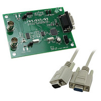
KIT EVAL FOR MAX7456
Manufacturer
Maxim Integrated Products
Specifications of MAX7456EVKIT+
Main Purpose
Video, On-Screen Display (OSD)
Embedded
Yes, MCU, 16-Bit
Utilized Ic / Part
MAX7456
Primary Attributes
NTSC/PAL single-channel monochrome on-screen display(OSD) with integrated video driver
Secondary Attributes
GUI, SPI Interfaces
Lead Free Status / RoHS Status
Lead free / RoHS Compliant


1, 2, 13–16,
27, 28
PIN
10
11
12
17
18
19
20
21
22
23
24
25
26
—
3
4
5
6
7
8
9
CLKOUT
SDOUT
HSYNC
VSYNC
RESET
NAME
DGND
CLKIN
AGND
PGND
DVDD
AVDD
PVDD
VOUT
SCLK
SDIN
SAG
N.C.
LOS
XFB
VIN
CS
EP
_______________________________________________________________________________________
Single-Channel Monochrome On-Screen
No Connection. Not internally connected.
Digital Power-Supply Input. Bypass to DGND with a 0.1µF capacitor.
Digital Ground
Crystal Connection 1. Connect a parallel resonant, fundamental mode crystal between CLKIN and XFB
for use as a crystal oscillator, or drive CLKIN directly with a 27MHz system reference clock.
Crystal Connection 2. Connect a parallel resonant, fundamental mode crystal between CLKIN and XFB
for use as a crystal oscillator, or leave XFB unconnected when driving CLKIN with a 27MHz system
reference clock.
Clock Output. 27MHz logic-level output system clock.
Active-Low Chip-Select Input. SDOUT goes high impedance when CS is high.
Serial Data Input. Data is clocked in at rising edge of SCLK.
Serial Clock Input. Clocks data into SDIN and out of SDOUT. Duty cycle must be between 40% and 60%.
Serial Data Output. Data is clocked out at the falling edge of SCLK. High impedance when CS is high.
Loss-of-Sync Output (Open-Drain). LOS goes high when the VIN sync pulse is lost for 32 consecutive
lines. LOS goes low when 32 consecutive valid sync pulses are received. Connect to a 1kΩ pullup
resistor to DVDD or another positive supply voltage suitable for the receiving device.
Vertical Sync Output (Open-Drain). VSYNC goes low following the video input’s vertical sync interval.
VSYNC is either recovered from VIN or internally generated when in internal sync mode. Connect to a
1kΩ pullup resistor to DVDD or another positive supply voltage suitable for the receiving device.
Horizontal Sync Output (Open-Drain). HSYNC goes low following the video input’s horizontal sync
interval. HSYNC is either recovered from VIN or internally generated when in internal sync mode. Connect
to a 1kΩ pullup resistor to DVDD or another positive supply voltage suitable for the receiving device.
System Reset Input. The minimum RESET pulse width is 50ms. All SPI registers are reset to their default
values after 100µs following the rising edge of RESET. These registers are not accessible for reading or
writing during that time. The display memory is reset to its default value of 00H in all locations after 20µs
following the rising edge of RESET.
Analog Ground
Analog Power-Supply Input. Bypass to AGND with a 0.1µF capacitor.
PAL or NTSC CVBS Video Input
Driver Ground. Connect to AGND at a single point.
Driver Power-Supply Input. Bypass to PGND with a 0.1µF capacitor.
Sag Correction Input. Connect to VOUT if not used. See Figure 1b.
Video Output
Exposed Pad. Internally connected to AGND. Connect EP to the AGND plane for improved heat
dissipation. Do not use EP as the only ground connection.
Display with Integrated EEPROM
FUNCTION
Pin Description
9
Related parts for MAX7456EVKIT+
Image
Part Number
Description
Manufacturer
Datasheet
Request
R

Part Number:
Description:
MAX7528KCWPMaxim Integrated Products [CMOS Dual 8-Bit Buffered Multiplying DACs]
Manufacturer:
Maxim Integrated Products
Datasheet:
Part Number:
Description:
Single +5V, fully integrated, 1.25Gbps laser diode driver.
Manufacturer:
Maxim Integrated Products
Datasheet:
Part Number:
Description:
Single +5V, fully integrated, 155Mbps laser diode driver.
Manufacturer:
Maxim Integrated Products
Datasheet:
Part Number:
Description:
VRD11/VRD10, K8 Rev F 2/3/4-Phase PWM Controllers with Integrated Dual MOSFET Drivers
Manufacturer:
Maxim Integrated Products
Datasheet:
Part Number:
Description:
Highly Integrated Level 2 SMBus Battery Chargers
Manufacturer:
Maxim Integrated Products
Datasheet:
Part Number:
Description:
Current Monitor and Accumulator with Integrated Sense Resistor; ; Temperature Range: -40°C to +85°C
Manufacturer:
Maxim Integrated Products
Part Number:
Description:
TSSOP 14/A�/RS-485 Transceivers with Integrated 100O/120O Termination Resis
Manufacturer:
Maxim Integrated Products
Part Number:
Description:
TSSOP 14/A�/RS-485 Transceivers with Integrated 100O/120O Termination Resis
Manufacturer:
Maxim Integrated Products
Part Number:
Description:
QFN 16/A�/AC-DC and DC-DC Peak-Current-Mode Converters with Integrated Step
Manufacturer:
Maxim Integrated Products
Part Number:
Description:
TDFN/A/65V, 1A, 600KHZ, SYNCHRONOUS STEP-DOWN REGULATOR WITH INTEGRATED SWI
Manufacturer:
Maxim Integrated Products
Part Number:
Description:
Integrated Temperature Controller f
Manufacturer:
Maxim Integrated Products
Part Number:
Description:
SOT23-6/I�/45MHz to 650MHz, Integrated IF VCOs with Differential Output
Manufacturer:
Maxim Integrated Products
Part Number:
Description:
SOT23-6/I�/45MHz to 650MHz, Integrated IF VCOs with Differential Output
Manufacturer:
Maxim Integrated Products
Part Number:
Description:
EVALUATION KIT/2.4GHZ TO 2.5GHZ 802.11G/B RF TRANSCEIVER WITH INTEGRATED PA
Manufacturer:
Maxim Integrated Products
Part Number:
Description:
QFN/E/DUAL PCIE/SATA HIGH SPEED SWITCH WITH INTEGRATED BIAS RESISTOR
Manufacturer:
Maxim Integrated Products
Datasheet: