MAX7456EVKIT+ Maxim Integrated Products, MAX7456EVKIT+ Datasheet - Page 5
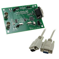
MAX7456EVKIT+
Manufacturer Part Number
MAX7456EVKIT+
Description
KIT EVAL FOR MAX7456
Manufacturer
Maxim Integrated Products
Specifications of MAX7456EVKIT+
Main Purpose
Video, On-Screen Display (OSD)
Embedded
Yes, MCU, 16-Bit
Utilized Ic / Part
MAX7456
Primary Attributes
NTSC/PAL single-channel monochrome on-screen display(OSD) with integrated video driver
Secondary Attributes
GUI, SPI Interfaces
Lead Free Status / RoHS Status
Lead free / RoHS Compliant


TIMING CHARACTERISTICS (continued)
(V
= V
Figure 1. Standard Test Circuits
Note 1: See the standard test circuits of Figure 1. R
Note 2: The input-voltage operating range is the input range over which the output signal parameters are guaranteed (Figure 3).
Note 3: The input-voltage sync detection range is the input composite video range over which an input sync signal is properly
VOUT Sync to VSYNC Rising
Edge Delay
VSYNC Falling Edge to VOUT
Sync Delay
VSYNC Rising Edge to VOUT
Sync Delay
VOUT Sync to HSYNC Falling
Edge Delay
VOUT Sync to HSYNC Rising
Edge Delay
HSYNC Falling Edge to VOUT
Sync Delay
HSYNC Rising Edge to VOUT
Sync Delay
All Supplies High to CS Low
NVM Write Busy
AVDD
DVDD
SIGNAL
GEN
= +4.75V to +5.25V, V
voltage level of (V
teed by design.
detected and the OSD signal appears at VOUT. However, the output voltage specifications are not guaranteed for input sig-
nals exceeding the maximum specified in the input operating voltage range (Figure 3).
= V
PARAMETER
PVDD
= +5V, T
75Ω
R
IN
_______________________________________________________________________________________
a) INPUT TEST CIRCUIT
Single-Channel Monochrome On-Screen
0.1μF
IH
A
C
IN
= +25°C, unless otherwise noted.) (Note 1)
+ V
DVDD
IL
VIN
) / 2. All parameters are tested at T
t
t
t
t
t
t
SYMBOL
t
= +4.75V to +5.25V, V
VOUT-HSR
HSR-VOUT
VOUT-VSR
VSF-VOUT
VSR-VOUT
VOUT-HSF
HSF-VOUT
t
t
NVW
PUD
MAX7456
Display with Integrated EEPROM
NTSC external sync mode, Figure 4
PAL external sync mode, Figure 6
NTSC internal sync mode, Figure 5
PAL internal sync mode, Figure 7
NTSC internal sync mode, Figure 5
PAL internal sync mode, Figure 7
NTSC and PAL external sync mode,
Figure 8
NTSC and PAL external sync mode,
Figure 8
NTSC and PAL internal sync mode,
Figure 9
NTSC and PAL internal sync mode,
Figure 9
Power-up delay
L
= 75Ω, unless otherwise specified. All digital input signals are timed from a
PVDD
CONDITIONS
= +4.75V to +5.25V, T
A
= +85°C and values through temperature range are guaran-
MAX7456
b) ONE STANDARD VIDEO LOAD, DC-COUPLED
A
= T
MIN
MIN
VOUT
to T
SAG
MAX
. Typical values are at V
TYP
400
425
310
325
115
115
40
45
32
30
50
12
C
22pF
MAX
L
R
150Ω
L
UNITS
ms
ms
ns
ns
ns
ns
ns
ns
ns
AVDD
5
Related parts for MAX7456EVKIT+
Image
Part Number
Description
Manufacturer
Datasheet
Request
R

Part Number:
Description:
MAX7528KCWPMaxim Integrated Products [CMOS Dual 8-Bit Buffered Multiplying DACs]
Manufacturer:
Maxim Integrated Products
Datasheet:
Part Number:
Description:
Single +5V, fully integrated, 1.25Gbps laser diode driver.
Manufacturer:
Maxim Integrated Products
Datasheet:
Part Number:
Description:
Single +5V, fully integrated, 155Mbps laser diode driver.
Manufacturer:
Maxim Integrated Products
Datasheet:
Part Number:
Description:
VRD11/VRD10, K8 Rev F 2/3/4-Phase PWM Controllers with Integrated Dual MOSFET Drivers
Manufacturer:
Maxim Integrated Products
Datasheet:
Part Number:
Description:
Highly Integrated Level 2 SMBus Battery Chargers
Manufacturer:
Maxim Integrated Products
Datasheet:
Part Number:
Description:
Current Monitor and Accumulator with Integrated Sense Resistor; ; Temperature Range: -40°C to +85°C
Manufacturer:
Maxim Integrated Products
Part Number:
Description:
TSSOP 14/A�/RS-485 Transceivers with Integrated 100O/120O Termination Resis
Manufacturer:
Maxim Integrated Products
Part Number:
Description:
TSSOP 14/A�/RS-485 Transceivers with Integrated 100O/120O Termination Resis
Manufacturer:
Maxim Integrated Products
Part Number:
Description:
QFN 16/A�/AC-DC and DC-DC Peak-Current-Mode Converters with Integrated Step
Manufacturer:
Maxim Integrated Products
Part Number:
Description:
TDFN/A/65V, 1A, 600KHZ, SYNCHRONOUS STEP-DOWN REGULATOR WITH INTEGRATED SWI
Manufacturer:
Maxim Integrated Products
Part Number:
Description:
Integrated Temperature Controller f
Manufacturer:
Maxim Integrated Products
Part Number:
Description:
SOT23-6/I�/45MHz to 650MHz, Integrated IF VCOs with Differential Output
Manufacturer:
Maxim Integrated Products
Part Number:
Description:
SOT23-6/I�/45MHz to 650MHz, Integrated IF VCOs with Differential Output
Manufacturer:
Maxim Integrated Products
Part Number:
Description:
EVALUATION KIT/2.4GHZ TO 2.5GHZ 802.11G/B RF TRANSCEIVER WITH INTEGRATED PA
Manufacturer:
Maxim Integrated Products
Part Number:
Description:
QFN/E/DUAL PCIE/SATA HIGH SPEED SWITCH WITH INTEGRATED BIAS RESISTOR
Manufacturer:
Maxim Integrated Products
Datasheet: