MAX7456EVKIT+ Maxim Integrated Products, MAX7456EVKIT+ Datasheet - Page 2
MAX7456EVKIT+
Manufacturer Part Number
MAX7456EVKIT+
Description
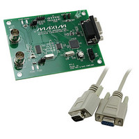
KIT EVAL FOR MAX7456
Manufacturer
Maxim Integrated Products
Specifications of MAX7456EVKIT+
Main Purpose
Video, On-Screen Display (OSD)
Embedded
Yes, MCU, 16-Bit
Utilized Ic / Part
MAX7456
Primary Attributes
NTSC/PAL single-channel monochrome on-screen display(OSD) with integrated video driver
Secondary Attributes
GUI, SPI Interfaces
Lead Free Status / RoHS Status
Lead free / RoHS Compliant


ABSOLUTE MAXIMUM RATINGS
AVDD to AGND ........................................................-0.3V to +6V
DVDD to DGND ........................................................-0.3V to +6V
PVDD to PGND.........................................................-0.3V to +6V
AGND to DGND.....................................................-0.3V to +0.3V
AGND to PGND .....................................................-0.3V to +0.3V
DGND to PGND.....................................................-0.3V to +0.3V
VIN, VOUT, SAG to AGND......................-0.3V to (V
HSYNC, VSYNC, LOS to AGND ...............................-0.3V to +6V
RESET to AGND .....................................-0.3V to (V
Single-Channel Monochrome On-Screen
Display with Integrated EEPROM
ELECTRICAL CHARACTERISTICS
(V
= V
* As per JEDEC51 Standard (Multilayer Board).
Stresses beyond those listed under “Absolute Maximum Ratings” may cause permanent damage to the device. These are stress ratings only, and functional
operation of the device at these or any other conditions beyond those indicated in the operational sections of the specifications is not implied. Exposure to
absolute maximum rating conditions for extended periods may affect device reliability.
2
POWER SUPPLIES
Analog Supply Voltage
Digital Supply Voltage
Driver Supply Voltage
Analog Supply Current
Digital Supply Current
Driver Supply Current
NONVOLATILE MEMORY
Data Retention
Endurance
DIGITAL INPUTS (CS, SDIN, RESET, SCLK)
Input High Voltage
Input Low Voltage
Input Hysteresis
Input Leakage Current
Input Capacitance
DIGITAL OUTPUTS (SDOUT, CLKOUT, VSYNC, HSYNC, LOS)
Output High Voltage
Output Low Voltage
Tri-State Leakage Current
AVDD
DVDD
_______________________________________________________________________________________
= +4.75V to +5.25V, V
= V
PARAMETER
PVDD
= +5V, T
A
= +25°C, unless otherwise noted.) (Note 1)
DVDD
SYMBOL
= +4.75V to +5.25V, V
V
V
V
I
I
I
V
DVDD
AVDD
PVDD
V
AVDD
DVDD
V
PVDD
C
V
V
HYS
OH
OL
IH
IL
IN
V
VOUT load, R
V
VOUT load, R
V
VOUT load, R
T
T
I
I
SDOUT, CS = V
V
SOURCE
SINK
A
A
IN
IN
IN
IN
AVDD
AVDD
= +25°C
= +25°C
= 1V
= 1V
= 1V
= 0 or V
= 4mA
+ 0.3V)
+ 0.3V)
P-P
P-P
P-P
= 4mA (SDOUT, CLKOUT)
PVDD
(100% white flat field signal),
(100% white flat field signal),
(100% white flat field signal),
DVDD
L
L
L
CONDITIONS
= 150Ω
= 150Ω
= 150Ω
DVDD
= +4.75V to +5.25V, T
CLKIN, CLKOUT, XFB to DGND ............-0.3V to (V
SDIN, SCLK, CS, SDOUT to DGND........-0.3V to (V
Maximum Continuous Current into V
Continuous Power Dissipation (T
Operating Temperature Range ...........................-40°C to +85°C
Junction Temperature ......................................................+150°C
Storage Temperature Range .............................-60°C to +150°C
Lead Temperature (soldering, 10s) .................................+300°C
28-Pin TSSOP (derate 27mW/°C above +70°C) .......2162mW*
A
= T
MIN
4.75
4.75
4.75
MIN
2.0
2.4
to T
MAX
A
100,000
= +70°C)
. Typical values are at V
TYP
100
OUT
24
25
58
50
5
5
5
5
........................±100mA
MAX
5.25
5.25
5.25
0.45
±10
±10
0.8
35
30
80
DVDD
DVDD
UNITS
Stores
Years
+ 0.3V)
+ 0.3V)
mA
mA
mA
mV
µA
µA
pF
V
V
V
V
V
V
V
AVDD
Related parts for MAX7456EVKIT+
Image
Part Number
Description
Manufacturer
Datasheet
Request
R

Part Number:
Description:
MAX7528KCWPMaxim Integrated Products [CMOS Dual 8-Bit Buffered Multiplying DACs]
Manufacturer:
Maxim Integrated Products
Datasheet:
Part Number:
Description:
Single +5V, fully integrated, 1.25Gbps laser diode driver.
Manufacturer:
Maxim Integrated Products
Datasheet:
Part Number:
Description:
Single +5V, fully integrated, 155Mbps laser diode driver.
Manufacturer:
Maxim Integrated Products
Datasheet:
Part Number:
Description:
VRD11/VRD10, K8 Rev F 2/3/4-Phase PWM Controllers with Integrated Dual MOSFET Drivers
Manufacturer:
Maxim Integrated Products
Datasheet:
Part Number:
Description:
Highly Integrated Level 2 SMBus Battery Chargers
Manufacturer:
Maxim Integrated Products
Datasheet:
Part Number:
Description:
Current Monitor and Accumulator with Integrated Sense Resistor; ; Temperature Range: -40°C to +85°C
Manufacturer:
Maxim Integrated Products
Part Number:
Description:
TSSOP 14/A�/RS-485 Transceivers with Integrated 100O/120O Termination Resis
Manufacturer:
Maxim Integrated Products
Part Number:
Description:
TSSOP 14/A�/RS-485 Transceivers with Integrated 100O/120O Termination Resis
Manufacturer:
Maxim Integrated Products
Part Number:
Description:
QFN 16/A�/AC-DC and DC-DC Peak-Current-Mode Converters with Integrated Step
Manufacturer:
Maxim Integrated Products
Part Number:
Description:
TDFN/A/65V, 1A, 600KHZ, SYNCHRONOUS STEP-DOWN REGULATOR WITH INTEGRATED SWI
Manufacturer:
Maxim Integrated Products
Part Number:
Description:
Integrated Temperature Controller f
Manufacturer:
Maxim Integrated Products
Part Number:
Description:
SOT23-6/I�/45MHz to 650MHz, Integrated IF VCOs with Differential Output
Manufacturer:
Maxim Integrated Products
Part Number:
Description:
SOT23-6/I�/45MHz to 650MHz, Integrated IF VCOs with Differential Output
Manufacturer:
Maxim Integrated Products
Part Number:
Description:
EVALUATION KIT/2.4GHZ TO 2.5GHZ 802.11G/B RF TRANSCEIVER WITH INTEGRATED PA
Manufacturer:
Maxim Integrated Products
Part Number:
Description:
QFN/E/DUAL PCIE/SATA HIGH SPEED SWITCH WITH INTEGRATED BIAS RESISTOR
Manufacturer:
Maxim Integrated Products
Datasheet: