LMK03200EVAL National Semiconductor, LMK03200EVAL Datasheet - Page 16
LMK03200EVAL
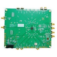
Manufacturer Part Number
LMK03200EVAL
Description
BOARD EVALUATION LMK03200
Manufacturer
National Semiconductor
Specifications of LMK03200EVAL
Main Purpose
Timing, Clock Conditioner
Embedded
No
Utilized Ic / Part
LMK03200
Primary Attributes
3 LVDS & 5 LVPECL Outputs, Integrated PLL & VCO
Secondary Attributes
3.15 V ~ 3.45 V Supply
Silicon Manufacturer
National
Silicon Core Number
LMK03200
Kit Application Type
Clock & Timing
Application Sub Type
Precision Clock Conditioner
Kit Contents
Board, Cable
Lead Free Status / RoHS Status
Lead free / RoHS Compliant


www.national.com
1.10 DIGITAL LOCK DETECT
The PLL digital lock detect circuitry compares the difference
between the phase of the inputs of the phase detector to a
RC generated delay of ε. To indicate a locked state the phase
error must be less than the ε RC delay for 5 consecutive ref-
erence cycles. Once in lock, the RC delay is changed to
approximately δ. To indicate an out of lock state, the phase
error must become greater δ. The values of ε and δ are shown
in the table below:
To utilize the digital lock detect feature, PLL_MUX must be
programmed for "Digital Lock Detect (Active High)" or "Digital
Lock Detect (Active Low)." When one of these modes is pro-
grammed the state of the LD pin will be set high or low as
determined by the description above as shown in
When the device is in power down mode and the LD pin is
programmed for a digital lock detect function, LD will show a
"no lock detected" condition which is low or high given active
high or active low circuitry respectively.
The accuracy of this circuit degrades at higher comparison
frequencies. To compensate for this, the DIV4 word should
be set to one if the comparison frequency exceeds 20 MHz.
The function of this word is to divide the comparison frequen-
cy presented to the lock detect circuit by 4.
10 ns
ε
20 ns
δ
Figure
3.
16
1.11 CLKout DELAYS
Each individual clock output includes a delay adjustment.
Clock output delay registers (CLKoutX_DLY) support a 150
ps step size and range from 0 to 2250 ps of total delay.
FIGURE 3. Digital Lock Detect Flowchart
30088705
Related parts for LMK03200EVAL
Image
Part Number
Description
Manufacturer
Datasheet
Request
R

Part Number:
Description:
Precision 0-delay Clock Conditioner With Integrated Vco
Manufacturer:
National Semiconductor Corporation
Datasheet:

Part Number:
Description:
National Semiconductor [8-Bit D/A Converter]
Manufacturer:
National Semiconductor
Datasheet:
Part Number:
Description:
National Semiconductor [Media Coprocessor]
Manufacturer:
National Semiconductor
Datasheet:
Part Number:
Description:
Digitally Controlled Tone and Volume Circuit with Stereo Audio Power Amplifier, Microphone Preamp Stage and National 3D Sound
Manufacturer:
National Semiconductor
Datasheet:
Part Number:
Description:
Digitally Controlled Tone and Volume Circuit with Stereo Audio Power Amplifier, Microphone Preamp Stage and National 3D Sound
Manufacturer:
National Semiconductor
Datasheet:
Part Number:
Description:
AC97 Rev 2 Codec with Sample Rate Conversion and National 3D Sound
Manufacturer:
National Semiconductor
Part Number:
Description:
Manufacturer:
National Semiconductor
Datasheet:
Part Number:
Description:
Manufacturer:
National Semiconductor
Datasheet:
Part Number:
Description:
General Purpose, Low Voltage, Low Power, Rail-to-Rail Output Operational Amplifiers
Manufacturer:
National Semiconductor
Datasheet:
Part Number:
Description:
8-bit 20 MSPS flash A/D converter.
Manufacturer:
National Semiconductor
Datasheet:
Part Number:
Description:
Low Noise Quad Operational Amplifier
Manufacturer:
National Semiconductor
Datasheet:
Part Number:
Description:
Quad Differential Line Receivers
Manufacturer:
National Semiconductor
Datasheet:
Part Number:
Description:
Quad High Speed Trapezoidal? Bus Transceiver
Manufacturer:
National Semiconductor
Datasheet:
Part Number:
Description:
Dual Line Receiver
Manufacturer:
National Semiconductor
Datasheet: