LMK03200EVAL National Semiconductor, LMK03200EVAL Datasheet - Page 10
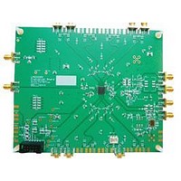
LMK03200EVAL
Manufacturer Part Number
LMK03200EVAL
Description
BOARD EVALUATION LMK03200
Manufacturer
National Semiconductor
Specifications of LMK03200EVAL
Main Purpose
Timing, Clock Conditioner
Embedded
No
Utilized Ic / Part
LMK03200
Primary Attributes
3 LVDS & 5 LVPECL Outputs, Integrated PLL & VCO
Secondary Attributes
3.15 V ~ 3.45 V Supply
Silicon Manufacturer
National
Silicon Core Number
LMK03200
Kit Application Type
Clock & Timing
Application Sub Type
Precision Clock Conditioner
Kit Contents
Board, Cable
Lead Free Status / RoHS Status
Lead free / RoHS Compliant


www.national.com
Jitter
V
ΔV
V
ΔV
I
I
I
Jitter
V
V
V
V
V
I
I
V
V
V
V
I
I
SA
SB
SAB
IH
IL
IH
IL
OD
OS
OH
OL
OD
IH
IL
OH
OL
IH
IL
Symbol
OD
OS
ADD
ADD
Additive RMS Jitter
Differential Output Voltage
Change in magnitude of V
complementary output states
Output Offset Voltage
Change in magnitude of V
complementary output states
Clock Output Short Circuit Current
single-ended
Clock Output Short Circuit Current
differential
Additive RMS Jitter
Output High Voltage
Output Low Voltage
Differential Output Voltage
High-Level Input Voltage
Low-Level Input Voltage
High-Level Input Current
Low-Level Input Current
High-Level Output Voltage
Low-Level Output Voltage
High-Level Input Voltage
Low-Level Input Voltage
High-Level Input Current
Low-Level Input Current
Parameter
Clock Distribution Section
(Note 12)
(Note 12)
Clock Distribution Section - LVDS Clock Outputs
OD
OS
for
for
Digital MICROWIRE Interfaces
Digital LVTTL Interfaces
R
Distribution Path =
765 MHz
Bandwidth =
12 kHz to 20 MHz
R
R
R
R
Single-ended outputs shorted to GND
Complementary outputs tied together
R
Distribution Path =
765 MHz
Bandwidth =
12 kHz to 20 MHz
Termination = 50 Ω to Vcc - 2 V
R
V
V
I
I
V
V
OH
OL
IH
IL
IH
IL
L
L
L
L
L
L
L
= 100 Ω
= 100 Ω
= 100 Ω
= 100 Ω
= 100 Ω
= 100 Ω
= 100 Ω
= -500 µA
= 0
= 0
= Vcc
= +500 µA
= Vcc
(Note 12)
10
Conditions
- LVPECL Clock Outputs
(Note 14)
(Note 15)
CLKoutX_MUX
= Bypass (no
divide or delay)
CLKoutX_MUX
= Divided (no
delay)
CLKoutX_DIV =
4
CLKoutX_MUX
= Bypass (no
divide or delay)
CLKoutX_MUX
= Divided (no
delay)
CLKoutX_DIV =
4
(Note 12)
1.070
-40.0
Vcc -
Min
-5.0
-5.0
-5.0
250
660
-50
-35
-24
-12
2.0
0.4
1.6
Vcc -
Vcc -
1.25
0.98
Typ
350
810
1.8
20
75
20
75
1.370
Max
450
965
Vcc
Vcc
0.8
5.0
5.0
0.4
0.4
5.0
5.0
50
35
24
12
Units
mV
mV
mV
mA
mA
mV
µA
µA
µA
µA
fs
fs
V
V
V
V
V
V
V
V
V
Related parts for LMK03200EVAL
Image
Part Number
Description
Manufacturer
Datasheet
Request
R

Part Number:
Description:
Precision 0-delay Clock Conditioner With Integrated Vco
Manufacturer:
National Semiconductor Corporation
Datasheet:

Part Number:
Description:
National Semiconductor [8-Bit D/A Converter]
Manufacturer:
National Semiconductor
Datasheet:
Part Number:
Description:
National Semiconductor [Media Coprocessor]
Manufacturer:
National Semiconductor
Datasheet:
Part Number:
Description:
Digitally Controlled Tone and Volume Circuit with Stereo Audio Power Amplifier, Microphone Preamp Stage and National 3D Sound
Manufacturer:
National Semiconductor
Datasheet:
Part Number:
Description:
Digitally Controlled Tone and Volume Circuit with Stereo Audio Power Amplifier, Microphone Preamp Stage and National 3D Sound
Manufacturer:
National Semiconductor
Datasheet:
Part Number:
Description:
AC97 Rev 2 Codec with Sample Rate Conversion and National 3D Sound
Manufacturer:
National Semiconductor
Part Number:
Description:
Manufacturer:
National Semiconductor
Datasheet:
Part Number:
Description:
Manufacturer:
National Semiconductor
Datasheet:
Part Number:
Description:
General Purpose, Low Voltage, Low Power, Rail-to-Rail Output Operational Amplifiers
Manufacturer:
National Semiconductor
Datasheet:
Part Number:
Description:
8-bit 20 MSPS flash A/D converter.
Manufacturer:
National Semiconductor
Datasheet:
Part Number:
Description:
Low Noise Quad Operational Amplifier
Manufacturer:
National Semiconductor
Datasheet:
Part Number:
Description:
Quad Differential Line Receivers
Manufacturer:
National Semiconductor
Datasheet:
Part Number:
Description:
Quad High Speed Trapezoidal? Bus Transceiver
Manufacturer:
National Semiconductor
Datasheet:
Part Number:
Description:
Dual Line Receiver
Manufacturer:
National Semiconductor
Datasheet: