CDB4265 Cirrus Logic Inc, CDB4265 Datasheet
CDB4265
Specifications of CDB4265


Related parts for CDB4265


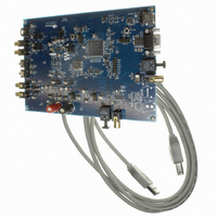
CDB4265 Summary of contents
Page 1
Stereo Audio CODEC D/A Features Multi-Bit Delta Sigma Modulator 104 dB Dynamic Range -90 dB THD 192 kHz Sampling Rates Single-Ended Analog Architecture Volume Control with Soft Ramp – 0.5 dB Step Size ...
Page 2
... CS4265 and other devices operating over a wide range of logic levels. The CS4265 is available in a 32-pin QFN package for both Commercial (-10° to +70° C) and Automotive (-40° to +105° C) grade. The CDB4265 is also available for device evaluation and implementation suggestions. Please refer to “Ordering Information” on page 56 complete details ...
Page 3
TABLE OF CONTENTS 1. PIN DESCRIPTIONS 2. CHARACTERISTICS AND SPECIFICATIONS ...................................................................................... 9 SPECIFIED OPERATING CONDITIONS ............................................................................................. 9 ABSOLUTE MAXIMUM RATINGS ....................................................................................................... 9 DAC ANALOG CHARACTERISTICS ................................................................................................. 10 DAC COMBINED INTERPOLATION & ON-CHIP ANALOG FILTER RESPONSE ............................ 11 ADC ANALOG CHARACTERISTICS ...
Page 4
DAC Digital Interface Format (Bits 5:4) ................................................................................. 36 6.3.2 Mute DAC (Bit 2) ................................................................................................................... 36 6.3.3 De-Emphasis Control (Bit 1) .................................................................................................. 37 6.4 ADC Control - Address 04h ............................................................................................................ 37 6.4.1 Functional Mode (Bits 7:6) .................................................................................................... 37 6.4.2 ADC ...
Page 5
Accessing the E Buffer ........................................................................................................ 53 11.2 Serial Copy Management System (SCMS) .................................................................................. 53 11.3 Channel Status Data E Buffer Access .......................................................................................... 53 11.3.1 One-Byte Mode ................................................................................................................... 54 11.3.2 Two-Byte Mode ................................................................................................................... 54 12. PACKAGE DIMENSIONS .................................................................................................................. 55 13. ...
Page 6
Figure 42.Consumer Output Circuit ( ........................................................................................ 51 Figure 43.TTL/CMOS Output Circuit ......................................................................................................... 51 Figure 44.Channel Status Data Buffer Structure ....................................................................................... 52 Figure 45.Flowchart for Writing the E Buffer ............................................................................................. 53 LIST OF TABLES Table 1. Speed Modes ...
Page 7
PIN DESCRIPTIONS SDA SCL VLC RESET VA AGND AINA AINB Pin Name # Pin Description SDA 1 Serial Control Data (Input/Output) - Bidirectional data line for the I²C control port. SCL 2 Serial Control Port Clock (Input) - Serial ...
Page 8
VA 17 Analog Power (Input) - Positive power for the internal analog section. AGND 18 Analog Ground (Input) - Ground reference for the internal analog section. AOUTA 19, 20 Analog Audio Output (Output) - The full scale output level is ...
Page 9
CHARACTERISTICS AND SPECIFICATIONS SPECIFIED OPERATING CONDITIONS AGND = DGND = 0 V; All voltages with respect to ground. Parameters DC Power Supplies: Ambient Operating Temperature (Power Applied) Notes: 1. Maximum of VA+0. 5.25 V, whichever is less. ...
Page 10
DAC ANALOG CHARACTERISTICS Test Conditions (unless otherwise specified): AGND = DGND = 0.25 V, whichever is less; VLS = VLC = ...
Page 11
Guaranteed by design. See maximum capacitance required for the internal op-amp’s stability. C internal output amp; increasing C DAC COMBINED INTERPOLATION & ON-CHIP ANALOG FILTER RESPONSE Parameter (Note 7,10) Combined Digital and On-chip Analog Filter Response Passband (Note 7) ...
Page 12
AOUTx R L AGND Figure 1. DAC Output Test Load 12 125 100 V 75 out 2 Figure 2. Maximum DAC Loading CS4265 Safe Operating Region Resistive Load -- ...
Page 13
ADC ANALOG CHARACTERISTICS Test conditions (unless otherwise specified): AGND = DGND = 0.25 V, whichever is less; VLS = VLC = ...
Page 14
Parameter Interchannel Isolation DC Accuracy Gain Error Gain Drift Line-Level Input Characteristics Full-scale Input Voltage Input Impedance Maximum Interchannel Input Impedance Mismatch Parameter DC Accuracy Interchannel Gain Mismatch Programmable Gain Characteristics Gain Step Size Absolute Gain Step Error 11. Valid ...
Page 15
ADC ANALOG CHARACTERISTICS (Continued) Parameter Dynamic Performance for 5.25 V Dynamic Range PGA Setting: - A-weighted unweighted PGA Setting: +12 dB A-weighted unweighted Total Harmonic Distortion + Noise (Note 12) PGA ...
Page 16
ADC DIGITAL FILTER CHARACTERISTICS Parameter (Notes 15, 17) Single-Speed Mode Passband (-0.1 dB) Passband Ripple Stopband Stopband Attenuation Total Group Delay (Fs = Output Sample Rate) Double-Speed Mode Passband (-0.1 dB) Passband Ripple Stopband Stopband Attenuation Total Group Delay (Fs ...
Page 17
DC ELECTRICAL CHARACTERISTICS AGND = DGND = 0 V, all voltages with respect to ground. MCLK=12.288 MHz; Fs=48 kHz; Master Mode. Parameter Power Supply Current (Normal Operation) Power Supply Current (Power-Down Mode) (Note 18) Power Consumption (Normal Operation) VA, VD, ...
Page 18
DIGITAL INTERFACE CHARACTERISTICS Test conditions (unless otherwise specified): AGND = DGND = 0 V; VLS = VLC = 1. 5.25 V. Parameters (Note 21) High-Level Input Voltage > 2.0 V Low-Level Input Voltage ...
Page 19
SWITCHING CHARACTERISTICS - SERIAL AUDIO PORT Logic ‘0’ = DGND = AGND = 0 V; Logic ‘1’ = VL, C Parameter Sample Rate MCLK Specifications MCLK Frequency MCLK Input Pulse Width High/Low MCLK Output Duty Cycle Master Mode LRCK Duty ...
Page 20
LRCK O utput SCLK O utput SDO UT SDIN Figure 3. Master Mode Serial Audio Port Timing LRCK Input SCLK Input SDOUT SDIN 20 t slr t sdo t sdis t t sclkh slr t sclkw t sdo t sdis ...
Page 21
Channel A - Left LRCK SCLK SDATA MSB - Figure 5. Format 0, Left-Justified up to 24-Bit Data Channel A - Left LRCK SCLK SDATA +5 +4 MSB - LRCK ...
Page 22
SWITCHING CHARACTERISTICS - I²C CONTROL PORT Inputs: Logic 0 = DGND = AGND = 0 V, Logic 1 = VLC, C Parameter SCL Clock Frequency RESET Rising Edge to Start Bus Free Time Between Transmissions Start Condition Hold Time (prior ...
Page 23
TYPICAL CONNECTION DIAGRAM +3.3V to +5V 10 µF +1.8V to +5V 0.1 µF 47 kΩ Note 4 Digital Audio Processor Digital Audio Output Micro- Controller 2 k Ω Ω +1.8V Note 1 to +5V 0.1 µF Note ...
Page 24
APPLICATIONS 4.1 Recommended Power-Up Sequence 1. Hold RESET low until the power supply,MCLK, and LRCK are stable. In this state, the Control Port is reset to its default settings. 2. Bring RESET high. The device will remain in a ...
Page 25
Master Mode As a clock master, LRCK and SCLK will operate as outputs. LRCK and SCLK are internally derived from MCLK with LRCK equal to Fs and SCLK equal shown in MCLK 4.2.3 Slave ...
Page 26
Analog Input Multiplexer, PGA, and Mic Gain The CS4265 contains a stereo 2-to-1 analog input multiplexer followed by a programmable gain amplifier (PGA). The input multiplexer is able to select either a line-level input source mic-level input ...
Page 27
If pseudo-differential input functionality is not required, simply connect the SGND pin to AGND through the parallel combination µF and a 0.1 µF capacitor 4.6 Output ...
Page 28
DAC outputs will always zero-data state. If non-zero serial audio input is present at the time of switching, a slight click or pop may be heard as the DAC output automatically goes to its ...
Page 29
Mute Control The MUTEC pin becomes active during power-up initialization, reset, muting, if the MCLK to LRCK ratio is incorrect, and during power-down. The MUTEC pin is intended to be used as control for an external mute circuit in ...
Page 30
The CS4265 also allows immediate muting of the IEC60958-3 transmit- ter audio data through a control register bit. External components are used to terminate and isolate the external cable from the CS4265. These ...
Page 31
SCL CHIP ADDRESS (WRITE AD0 0 SDA START SCL CHIP ADDRESS (WRITE) SDA ...
Page 32
Reset When RESET is low, the CS4265 enters a low-power mode and all internal states are reset, including the control port and registers, the outputs are muted. When RESET is high, the control port becomes operation- al, and the ...
Page 33
REGISTER QUICK REFERENCE This table shows the register names and their associated default values. Addr Function 7 01h Chip ID PART3 PART2 1 02h Power Control Freeze Reserved Reserved Reserved 0 03h DAC Control 1 Reserved Reserved DAC_DIF1 DAC_DIF0 ...
Page 34
Addr Function 7 11h Transmitter Reserved Control 1 0 12h Transmitter Tx_DIF1 Tx_DIF0 Control 2 0 13h - C-Data Buffer - 2Ah EFTCI CAM Reserved Reserved TxOff TxMute ...
Page 35
REGISTER DESCRIPTION 6.1 Chip ID - Register 01h 7 6 PART3 PART2 PART1 Function: This register is Read-Only. Bits 7 through 4 are the part number ID, which is 1101b (0Dh), and the remaining bits (3 through 0) indicate ...
Page 36
Power-Down DAC (Bit 1) Function: The DAC pair will remain in a reset state whenever this bit is set. 6.2.5 Power-Down Device (Bit 0) Function: The device will enter a low-power state whenever this bit is set. The power-down ...
Page 37
De-Emphasis Control (Bit 1) Function: The standard 50/15 μs digital de-emphasis filter response, rate of 44.1 kHz when the DeEmph bit is configured as shown in only in Single-Speed Mode. -10dB 6.4 ADC Control - Address 04h 7 6 ...
Page 38
ADC_DIF 0 Left-Justified 24-bit data (default) 1 6.4.3 Mute ADC (Bit 2) Function: When this bit is set, the serial audio output of the both ADC channels is muted. 6.4.4 ADC High-Pass Filter Freeze (Bit 1) Function: When ...
Page 39
Signal Selection - Address 06h 7 6 SDINSel Reserved Reserved 6.6.1 DAC SDIN Source (Bit 7) Function: This bit is used to select the serial audio data source for the DAC as shown in 6.6.2 Digital Loopback (Bit 1) ...
Page 40
ADC Input Control - Address 09h 7 6 Reserved Reserved Reserved 6.9.1 PGA Soft Ramp or Zero Cross Enable (Bits 4:3) Function: Soft Ramp Enable Soft Ramp allows level changes, both muting and attenuation implemented by incrementally ...
Page 41
DAC Channel B Volume Control - Address 0Bh 7 6 Vol7 Vol6 Vol5 6.11.1 Volume Control (Bits 7:0) Function: The digital volume control allows the user to attenuate the signal in 0.5 dB increments from 0 to -127 dB. ...
Page 42
The zero cross function is independently mon- itored and implemented for each channel. See DACSoft Table 16. DAC Soft Cross or Zero Cross Mode Selection ...
Page 43
Status Mask - Address 0Eh 7 6 Reserved Reserved Reserved Function: The bits of this register serve as a mask for the Status sources found in the register on page 42 mask bit is set to 1, ...
Page 44
Transmitter Control 2 - Address 12h 7 6 Tx_DIF1 Tx_DIF0 TxOff 6.18.1 Transmitter Digital Interface Format (Bits 7:6) Function: The required relationship between LRCK, SCLK and SDIN for the transmitter is defined by the Transmitter Digital Interface Format and ...
Page 45
Mono Mode Channel Selection (Bit 0) Function: When this bit is cleared, channel A input data will be transmitted in both channel A and B subframes in mono mode. When this bit is set, channel B input data will ...
Page 46
PARAMETER DEFINITIONS Dynamic Range The ratio of the rms value of the signal to the rms sum of all other spectral components over the specified bandwidth. Dynamic Range is a signal-to-noise ratio measurement over the specified bandwidth made with ...
Page 47
DAC FILTER PLOTS Figure 18. DAC Single-Speed Stopband Rejection -10 0.45 0.46 0.47 0.48 0.49 0.5 0.51 Frequency (normalized to Fs) Figure 20. DAC Single-Speed Transition Band Figure 22. ...
Page 48
Frequency (normalized to Fs) Figure 24. DAC Double-Speed Transition Band 0 ...
Page 49
ADC FILTER PLOTS 0 -10 -20 -30 -40 -50 -60 -70 -80 -90 -100 -110 -120 -130 -140 0.0 0.1 0.2 0.3 0.4 0.5 Frequency (norm alized to Fs) Figure 30. ADC Single-Speed Stopband Rejection ...
Page 50
Frequency (norm alized to Fs) Figure 36. ADC Double-Speed Transition Band (Detail) 0 -10 -20 -30 -40 -50 -60 -70 -80 -90 -100 -110 -120 ...
Page 51
IEC60958-3 TRANSMITTER COMPONENTS This section details the external components required to interface the IEC60958-3 transmitter to cables and fiber- optic components. 10.1 IEC60958-3 Transmitter External Components The IEC60958-3 specifications call for an unbalanced drive circuit with an output impedance ...
Page 52
STATUS BUFFER MANAGEMENT The CS4265 has a comprehensive channel status (C) data buffering scheme which allows the user to manage the C data through the control port. 11.1 IEC60958-3 Channel Status (C) Bit Management The CS4265 contains sufficient RAM ...
Page 53
Accessing the E Buffer The user can monitor the data being transferred by reading the E buffer, which is mapped into the register space of the CS4265, through the control port. The user can modify the data to be ...
Page 54
One-Byte Mode In many applications, the channel status blocks for the A and B channels will be identical. In this situation, if the user reads a byte from one of the channel's blocks, the corresponding byte for the other ...
Page 55
DIMENSIONS 32L QFN ( BODY) PACKAGE DRAWING D Pin #1 Corner Top View INCHES DIM MIN 0.0000 b 0.0071 0.0091 D 0.1969 BSC D2 0.1280 0.1299 E 0.1969 BSC E2 0.1280 0.1299 e ...
Page 56
... CS4265 Container Order # Tube CS4265-CNZ -10° to +70° C Tape & Reel CS4265-CNZR Tube CS4265-DNZ Tape & Reel CS4265-DNZR - - CDB4265 I²C Control Port Description and Timing description on page 35. table on page ADC Analog Characteristics table on page 19. and Channel A PGA Control - Address 08h 17. ...