STEVAL-ISF001V1 STMicroelectronics, STEVAL-ISF001V1 Datasheet - Page 23
STEVAL-ISF001V1
Manufacturer Part Number
STEVAL-ISF001V1
Description
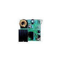
BOARD EVAL FOR L6563/STW55NM60N
Manufacturer
STMicroelectronics
Type
MOSFET & Power Driverr
Datasheets
1.STW55NM60N.pdf
(12 pages)
2.L6563ATR.pdf
(39 pages)
3.STEVAL-ISF001V1.pdf
(20 pages)
4.STEVAL-ISF001V1.pdf
(4 pages)
Specifications of STEVAL-ISF001V1
Main Purpose
Power Management, Power Factor Correction
Embedded
No
Utilized Ic / Part
L6563
Primary Attributes
3 kW, 400 V Out, FOT(Fixed Off Time Control), 240 VAC (185 ~ 265 Vrms)
Secondary Attributes
Iout Max 7.5 A
Product
Power Management Modules
Lead Free Status / RoHS Status
Lead free / RoHS Compliant
For Use With/related Products
STW55NM60N
Other names
497-8850


L6563 - L6563A
6.5
Tracking Boost function
In some applications it may be advantageous to regulate the output voltage of the PFC pre-
regulator so that it tracks the RMS input voltage rather than at a fixed value like in
conventional boost pre-regulators. This is commonly referred to as "tracking boost" or
"follower boost" approach.
With this IC the function can be realized by connecting a resistor (R
and ground. The TBO pin presents a DC level equal to the peak of the MULT pin voltage and
is then representative of the mains RMS voltage. The resistor defines a current, equal to
V(TBO)/R
amplifier. In this way, when the mains voltage increases the voltage at TBO pin will increase
as well and so will do the current flowing through the resistor connected between TBO and
GND. Then a larger current will be sunk by INV pin and the output voltage of the PFC pre-
regulator will be forced to get higher. Obviously, the output voltage will move in the opposite
direction if the input voltage decreases.
To avoid undesired output voltage rise should the mains voltage exceed the maximum
specified value, the voltage at the TBO pin is clamped at 3V. By properly selecting the
multiplier bias it is possible to set the maximum input voltage above which input-to-output
tracking ends and the output voltage becomes constant. If this function is not used, leave
the pin open: the device will regulate a fixed output voltage.
Starting from the following data:
●
●
●
●
●
●
Vin
Vin
Vo
Vo
Vox = absolute maximum limit for the regulated output voltage;
∆Vo = OVP threshold,
1
2
1
2
= regulated output voltage @ Vin = Vin
= regulated output voltage @ Vin = Vin
= minimum specified input RMS voltage;
= maximum specified input RMS voltage;
T
, that is internally 1:1 mirrored and sunk from pin INV (pin 1) input of the error
1
2
;
;
Application information
T
) between the TBO pin
23/39
Related parts for STEVAL-ISF001V1
Image
Part Number
Description
Manufacturer
Datasheet
Request
R

Part Number:
Description:
BOARD RGB CTR ST7,STP08C596MTR
Manufacturer:
STMicroelectronics
Datasheet:

Part Number:
Description:
Power Management IC Development Tools Full Speed USB to RS232 Bridge Demo
Manufacturer:
STMicroelectronics
Datasheet:
Part Number:
Description:
Power Management IC Development Tools 2.5W solar eval BRD USB SPV1040 LD39050
Manufacturer:
STMicroelectronics
Datasheet:

Part Number:
Description:
BOARD EVAL FOR MEMS SENSORS
Manufacturer:
STMicroelectronics
Datasheet:

Part Number:
Description:
KIT DEV STARTER ST10F276Z5
Manufacturer:
STMicroelectronics
Datasheet:

Part Number:
Description:
BOARD EVAL HDMI $ VIDEO SWITCH
Manufacturer:
STMicroelectronics
Datasheet:

Part Number:
Description:
BOARD DEMO ACCELEROMETER DIL24
Manufacturer:
STMicroelectronics
Datasheet:

Part Number:
Description:
BOARD STLM75/STDS75/ST72F651
Manufacturer:
STMicroelectronics
Datasheet:

Part Number:
Description:
EVAL BOARD 3AXIS MEMS ACCELLRMTR
Manufacturer:
STMicroelectronics
Datasheet:

Part Number:
Description:
BOARD EVAL 8BIT MICRO + TDE1708
Manufacturer:
STMicroelectronics
Datasheet:
Part Number:
Description:
STMicroelectronics [RIPPLE-CARRY BINARY COUNTER/DIVIDERS]
Manufacturer:
STMicroelectronics
Datasheet:
Part Number:
Description:
STMicroelectronics [LIQUID-CRYSTAL DISPLAY DRIVERS]
Manufacturer:
STMicroelectronics
Datasheet:
Part Number:
Description:
BOARD EVAL FOR MEMS SENSORS
Manufacturer:
STMicroelectronics
Datasheet: