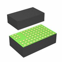
LTM8032IV#PBF Linear Technology, LTM8032IV#PBF Datasheet - Page 3

LTM8032IV#PBF
Manufacturer Part Number
LTM8032IV#PBF
Description
IC BUCK ADJ 2A 71LGA
Manufacturer
Linear Technology
Series
µModuler
Type
Point of Load (POL) Non-Isolatedr
Datasheet
1.LTM8032EVPBF.pdf
(20 pages)
Specifications of LTM8032IV#PBF
Design Resources
LTM8032 Spice Model
Output
0.8 ~ 10 V
Number Of Outputs
1
Power (watts)
20W
Mounting Type
Surface Mount
Voltage - Input
3.6 ~ 36 V
Package / Case
71-LGA
1st Output
0.8 ~ 10 VDC @ 2A
Size / Dimension
0.59" L x 0.35" W x 0.11" H (15mm x 9mm x 2.8mm)
Power (watts) - Rated
20W
Operating Temperature
-40°C ~ 125°C
Approvals
EN
Lead Free Status / RoHS Status
Lead free / RoHS Compliant
3rd Output
-
2nd Output
-
Available stocks
Company
Part Number
Manufacturer
Quantity
Price
ELECTRICAL CHARACTERISTICS
temperature range, otherwise specifi cations are at T
SYMBOL
V
V
I
I
I
ΔV
V
f
V
V
I
I
V
V
V
I
I
V
V
I
V
Note 1: Stresses beyond those listed under Absolute Maximum Ratings
may cause permanent damage to the device. Exposure to any Absolute
Maximum Rating condition for extended periods may affect device
reliability and lifetime.
Note 2: The LTM8032E is guaranteed to meet performance specifi cations
from 0°C to 125°C internal. Specifi cations over the –40°C to 125°C
internal temperature range are assured by design, characterization and
correlation with statistical process controls. LTM8032I is guaranteed
OUT
Q(VIN)
Q(BIAS)
V
SW
ADJ
RUN/SS
PGO
PGSINK
SYNC(BIAS)
ADJ
IN
OUT
OUT(AC_RMS)
BIAS(MIN)
IH(RUN/SS)
IL(RUN/SS)
PG(TH)
SYNCIL
SYNCIH
IN(RIPPLE)
OUT
OUT
PARAMETER
Input DC Voltage
Output DC Voltage
Continuous Output DC Current
V
BIAS Quiescent Current
Line Regulation
Load Regulation
Output Ripple (RMS)
Switching Frequency
Voltage at ADJ Pin
Minimum BIAS Voltage for Proper Operation
Current Out of ADJ Pin
RUN/SS Pin Current
RUN/SS Input High Voltage
RUN/SS Input Low Voltage
ADJ Voltage Threshold for PGOOD to Switch
PGOOD Leakage
PGOOD Sink Current
SYNC Input Low Threshold
SYNC Input High Threshold
SYNC Pin Bias Current
550kHz Narrowband Conducted Emission
1MHz Narrowband Conducted Emission
3MHz Narrowband Conducted Emission
IN
Quiescent Current
A
CONDITIONS
0.2A < I
0.2A < I
V
V
V
V
V
V
V
10V ≤ V
V
V
R
V
V
V
V
f
f
V
V
5μH LISN
= 25°C. V
SYNC
SYNC
IN
RUN/SS
BIAS
BIAS
RUN/SS
BIAS
BIAS
IN
IN
RUN/SS
RUN/SS
PG
PG
SYNC
IN
T
= 113k
= 24V
= 24V, 0.2A ≤ I
= 24V, I
= 24V, V
= 30V
= 0.4V
The
= 3V, Not Switching
= 0V, Not Switching
= 3V, Not Switching
= 0V, Not Switching
= 550kHz
= 550kHz
= 0V, V
OUT
OUT
IN
= 0.2V
= 0.2V
= 0V, V
= 2.5V
≤ 36V, I
l
IN
OUT
≤ 2A, R
≤ 2A, R
OUT
denotes the specifi cations which apply over the full operating
BIAS
= 10V, V
= 2A, V
ADJ
= 3.3V, I
OUT
= 0V
to meet specifi cations over the full –40°C to 125°C internal operating
temperature range. The LTM8032MP is guaranteed to meet specifi cations
over the full –55°C to 125°C internal operating temperature range. Note
that the maximum internal temperature is determined by specifi c operating
conditions in conjunction with board layout, the rated package thermal
resistance and other environmental factors.
Note 3: See Linear Technology Application Note 100.
OUT
= 0V, V
ADJ
ADJ
= 1A, V
≤ 2A, V
OUT
RUN/SS
Open
= 21.6k
OUT
OUT
= 3.3V
= 2A, f
OUT
OUT
= 1V
= 10V, V
= 3.3V
= 3.3V
SW
= 550kHz,
BIAS
= 3V, unless otherwise specifi ed.
l
l
l
l
MIN
765
200
3.6
2.5
0.7
0.03
TYP
325
790
730
800
0.8
0.6
0.1
0.3
1.9
0.1
0.1
10
25
88
60
89
69
51
1
6
4
5
LTM8032
MAX
120
120
815
2.8
0.2
0.5
36
60
10
2
5
1
UNITS
8032fc
dBμV
dBμV
dBμV
3
kHz
mV
mV
mV
μA
μA
μA
μA
μA
μA
μA
μA
μA
μA
μA
%
%
V
V
V
A
V
V
V
V
V


