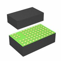
LTM8032IV#PBF Linear Technology, LTM8032IV#PBF Datasheet - Page 12

LTM8032IV#PBF
Manufacturer Part Number
LTM8032IV#PBF
Description
IC BUCK ADJ 2A 71LGA
Manufacturer
Linear Technology
Series
µModuler
Type
Point of Load (POL) Non-Isolatedr
Datasheet
1.LTM8032EVPBF.pdf
(20 pages)
Specifications of LTM8032IV#PBF
Design Resources
LTM8032 Spice Model
Output
0.8 ~ 10 V
Number Of Outputs
1
Power (watts)
20W
Mounting Type
Surface Mount
Voltage - Input
3.6 ~ 36 V
Package / Case
71-LGA
1st Output
0.8 ~ 10 VDC @ 2A
Size / Dimension
0.59" L x 0.35" W x 0.11" H (15mm x 9mm x 2.8mm)
Power (watts) - Rated
20W
Operating Temperature
-40°C ~ 125°C
Approvals
EN
Lead Free Status / RoHS Status
Lead free / RoHS Compliant
3rd Output
-
2nd Output
-
Available stocks
Company
Part Number
Manufacturer
Quantity
Price
APPLICATIONS INFORMATION
LTM8032
Synchronization
The internal oscillator of the LTM8032 can be synchro-
nized by applying an external 250kHz to 2MHz clock to
the SYNC pin. Do not leave this pin fl oating. The resistor
tied from the RT pin to ground should be chosen such
that the LTM8032 oscillates 20% lower than the intended
synchronization frequency (see the Frequency Selection
section). The LTM8032 will not enter Burst Mode operation
while synchronized to an external clock, but will instead
skip pulses to maintain regulation.
Shorted Input Protection
Care needs to be taken in systems where the output will
be held high when the input to the LTM8032 is absent.
This may occur in battery charging applications or in
battery back-up systems where a battery or some other
supply is diode ORed with the LTM8032’s output. If the
V
(either by a logic signal or because it is tied to V
the LTM8032’s internal circuitry will pull its quiescent
current through its internal power switch. This is fi ne if
your system can tolerate a few milliamps in this state. If
you ground the RUN/SS pin, the internal switch current
will drop to essentially zero. However, if the V
grounded while the output is held high, then parasitic
diodes inside the LTM8032 can pull large currents from
the output through the V
device. Figure 3 shows a circuit that will run only when
the input voltage is present and that protects against a
shorted or reversed input.
12
0.22μF
IN
RUN
15k
pin is allowed to fl oat and the RUN/SS pin is held high
Figure 2. To Soft-Start the LTM8032, Add a Resistor
and Capacitor to the RUN/SS Pin
RUN/SS
GND
IN
pin, potentially damaging the
2ms/DIV
8023 F02
IN
IN
), then
pin is
I
1A/DIV
V
2V/DIV
V
2V/DIV
L
RUN/SS
OUT
PCB Layout
Most of the headaches associated with PCB layout have
been alleviated or even eliminated by the high level of
integration of the LTM8032. The LTM8032 is neverthe-
less a switching power supply and care must be taken to
minimize EMI and ensure proper operation. Even with the
high level of integration, you may fail to achieve specifi ed
operation with a haphazard or poor layout. See Figure 4
for a suggested layout.
Ensure that the grounding and heat sinking are acceptable.
A few rules to keep in mind are:
1. Place the R
2. Place the C
3. Place the C
4. Place the C
5. Connect all of the GND connections to as large a copper
their respective pins.
and GND connection of the LTM8032. If a capacitor
is connected to the FIN terminals, place it as close
as possible to the FIN terminals, such that its ground
connection is as close as possible to that of the C
capacitor.
V
ground currents fl ow directly adjacent or underneath
the LTM8032.
pour or plane area as possible on the top layer. Avoid
breaking the ground connection between the external
components and the LTM8032.
Figure 3. The Input Diode Prevents a Shorted Input from
Discharging a Back-Up Battery Tied to the Output. It Also
Protects the Circuit from a Reversed Input. The LTM8032
Runs Only When the Input is Present
OUT
V
IN
and GND connection of the LTM8032.
ADJ
IN
OUT
IN
capacitor as close as possible to the V
and R
and C
capacitor as close as possible to the
T
OUT
V
RUN/SS
resistors as close as possible to
IN
R
T
LTM8032
SYNC
capacitors such that their
GND
V
BIAS
AUX
ADJ
OUT
8032 F03
V
OUT
8032fc
IN
IN


