FOD817A300W Fairchild Optoelectronics Group, FOD817A300W Datasheet
FOD817A300W
Specifications of FOD817A300W
Available stocks


Related parts for FOD817A300W


FOD817A300W Summary of contents
Page 1
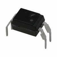
FOD814 Series, FOD817 Series 4-Pin High Operating Temperature Phototransistor Optocouplers Features AC input response (FOD814 only) Applicable to Pb-free IR reflow soldering Compact 4-pin package Current transfer ratio in selected groups: FOD814: 20–300% FOD817: 50–600% FOD814A: 50–150% FOD817A: 80–160% FOD817B: ...
Page 2
Absolute Maximum Ratings Stresses exceeding the absolute maximum ratings may damage the device. The device may not function or be operable above the recommended operating conditions and stressing the parts to these levels is not recommended. In addition, extended exposure ...
Page 3
Electrical Characteristics Individual Component Characteristics Symbol Parameter EMITTER V Forward Voltage F I Reverse Leakage Current R C Terminal Capacitance t DETECTOR I Collector Dark Current CEO BV Collector-Emitter Breakdown CEO Voltage BV Emitter-Collector Breakdown ECO Voltage DC Transfer Characteristics ...
Page 4
Electrical Characteristics Isolation Characteristics Symbol Characteristic V Input-Output Isolation ISO (3) Voltage R Isolation Resistance ISO C Isolation Capacitance ISO *Typical values 25°C A Notes: 1. Current Transfer Ratio (CTR For test circuit setup ...
Page 5
Typical Electrical/Optical Characteristics Fig. 1 Collector Power Dissipation vs. Ambient Temperature (FOD814) 200 150 100 50 0 -55 -40 - 100 120 AMBIENT TEMPERATURE T Fig. 3 Collector-Emitter Saturation Voltage vs. Forward Current 6 Ic ...
Page 6
Typical Electrical/Optical Characteristics Fig. 7 Collector Current vs. Collector-Emitter Voltage (FOD814 30mA AX.) 30 10mA 20 5mA ...
Page 7
Typical Electrical/Optical Characteristics Fig. 13 Response Time vs. Load Resistance 100 Ic= 2mA Ta = 25° 0.5 0.2 0.1 0.1 0.2 0.5 1 LOAD RESISTANCE ...
Page 8
Package Dimensions Through Hole 0.200 (5.10) 0.161 (4.10) 0.157 (4.00) 0.118 (3.00) 0.130 (3.30) 0.020 (0.51) 0.091 (2.30) TYP 0.150 (3.80) 0.110 (2.80) 0.024 (0.60) 0.016 (0.40) 0.110 (2.79) 0.090 (2.29) 0.4" Lead Spacing 0.200 (5.10) 0.157 (4.00) 0.161 (4.10) ...
Page 9
Ordering Information Option Part Number Example S SD FOD814SD 300 FOD814300 300W FOD814300W 3S FOD8143S 3SD FOD8143SD Marking Information Definitions ©2006 Fairchild Semiconductor Corporation FOD814 Series, FOD817 Series Rev. 1.1.4 FOD814S VDE Approved, 0.4" ...
Page 10
Carrier Tape Specifications Ø1.55 0.05 Note: All dimensions are in millimeters. Symbol W Tape wide P Pitch of sprocket holes 0 F Distance of compartment Distance of compartment to compartment 1 A0 Compartment B0 K0 ©2006 Fairchild ...
Page 11
Lead Free Recommended IR Reflow Condition Tp Tsmax Tsmin 25 C Profile Feature Preheat condition (Tsmin-Tsmax / ts) Melt soldering zone Peak temperature (Tp) Ramp-down rate Recommended Wave Soldering condition Profile Feature Peak temperature (Tp) ©2006 Fairchild Semiconductor Corporation FOD814 ...
Page 12
TRADEMARKS The following includes registered and unregistered trademarks and service marks, owned by Fairchild Semiconductor and/or its global subsidiaries, and is not intended exhaustive list of all such trademarks. Auto-SPM™ F-PFS™ FRFET Build it Now™ CorePLUS™ Global ...