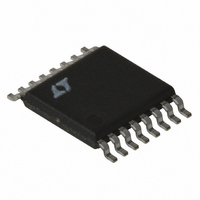
LT3430IFE Linear Technology, LT3430IFE Datasheet - Page 21

LT3430IFE
Manufacturer Part Number
LT3430IFE
Description
IC REG SW STDN 3A 200KHZ 16TSSOP
Manufacturer
Linear Technology
Type
Step-Down (Buck)r
Datasheet
1.LT3430EFE-1PBF.pdf
(28 pages)
Specifications of LT3430IFE
Internal Switch(s)
Yes
Synchronous Rectifier
No
Number Of Outputs
1
Voltage - Output
1.2 ~ 54 V
Current - Output
3A
Frequency - Switching
200kHz
Voltage - Input
5.5 ~ 60 V
Operating Temperature
-40°C ~ 125°C
Mounting Type
Surface Mount
Package / Case
16-TSSOP Exposed Pad, 16-eTSSOP, 16-HTSSOP
Lead Free Status / RoHS Status
Contains lead / RoHS non-compliant
Power - Output
-
Available stocks
Company
Part Number
Manufacturer
Quantity
Price
Part Number:
LT3430IFE
Manufacturer:
LT/凌特
Quantity:
20 000
Company:
Part Number:
LT3430IFE#PBF
Manufacturer:
LT
Quantity:
1 030
Part Number:
LT3430IFE#TRPB
Manufacturer:
LT
Quantity:
20 000
Part Number:
LT3430IFE-1
Manufacturer:
LINEAR/凌特
Quantity:
20 000
Company:
Part Number:
LT3430IFE-1#PBF
Manufacturer:
LT
Quantity:
973
Company:
Part Number:
LT3430IFETR
Manufacturer:
TOSH
Quantity:
4 574
Company:
Part Number:
LT3430IFETRPBF
Manufacturer:
LT
Quantity:
5 574
APPLICATIONS INFORMATION
ings = 0.233W • 45°C/W = 11°C. The 7V zener should be
sized for excess of 0.233W operaton. The tolerances of
the zener should be considered to ensure minimum V
exceeds 3.3V + V
Input Voltage vs Operating Frequency Considerations
The absolute maximum input supply voltage for the LT3430/
LT3430-1 is specifi ed at 60V. This is based solely on internal
semiconductor junction breakdown effects. Due to internal
power dissipation, the actual maximum V
a particular application may be less than this.
A detailed theoretical basis for estimating internal power
loss is given in the section, Thermal Considerations. Note
that AC switching loss is proportional to both operating
frequency and output current. The majority of AC switching
loss is also proportional to the square of input voltage.
For example, while the combination of V
= 5V at 2A and f
simultaneously raising V
not possible. Nevertheless, input voltage transients up to
60V can usually be accommodated, assuming the result-
ing increase in internal dissipation is of insuffi cient time
duration to raise die temperature signifi cantly.
A second consideration is controllability. A potential limita-
tion occurs with a high step-down ratio of V
this requires a correspondingly narrow minimum switch
on time. An approximate expression for this (assuming
continuous mode operation) is given as follows:
where:
A potential controllability problem arises if the LT3430/
LT3430-1 are called upon to produce an on time shorter
than it is able to produce. Feedback loop action will lower
then reduce the V
some sort of cycle-skipping or odd/even cycle behavior
is exhibited.
V
V
V
f
min t
OSC
IN
OUT
F
= Schottky diode forward drop
= input voltage
= switching frequency
ON
= output voltage
=
V
V
OUT
IN OSC
OSC
( )
DROOP
f
C
+
= 200kHz may be easily achievable,
V
control voltage to the point where
F
.
IN
to 60V and f
OSC
IN
IN
IN
achievable in
to 700kHz is
= 40V, V
to V
OUT
OUT
, as
C2
In summary:
1. Be aware that the simultaneous requirements of high
2. The simultaneous requirements of high V
FREQUENCY COMPENSATION
Before starting on the theoretical analysis of frequency
response, the following should be remembered—the
worse the board layout, the more diffi cult the circuit will
be to stabilize. This is true of almost all high frequency
analog circuits, read the Layout Considerations section
fi rst. Common layout errors that appear as stability prob-
lems are distant placement of input decoupling capacitor
and/or catch diode, and connecting the V
to a ground track carrying signifi cant switch current. In
addition, the theoretical analysis considers only fi rst
order non-ideal component behavior. For these reasons,
it is important that a fi nal stability check is made with
production layout and components.
The LT3430/LT3430-1 use current mode control. This al-
leviates many of the phase shift problems associated with
the inductor. The basic regulator loop is shown in Figure
10. The LT3430/LT3430-1 can be considered as two g
blocks, the error amplifi er and the power stage.
Figure 11 shows the overall loop response. At the V
pin, the frequency compensation components used are:
R
capacitor used is a 100µF, 10V tantalum capacitor with
typical ESR of 100mΩ. LT3430-1 uses two of these
capacitors in parallel.
The ESR of the tantalum output capacitor provides a use-
ful zero in the loop frequency response for maintaining
C
V
practice due to internal dissipation. The Thermal Con-
siderations section offers a basis to estimate internal
power. In questionable cases a prototype supply should
be built and exercised to verify acceptable operation.
high f
switch on time. Cycle skipping and/or odd/even cycle
behavior will result although correct output voltage is
usually maintained. The LT3430-1 100kHz switching
frequency will allow higher V
pulse skipping.
= 3.3k, C
IN
, high I
OSC
can result in an unacceptably short minimum
OUT
C
= 0.022µF and C
and high f
LT3430/LT3430-1
OSC
may not be achievable in
F
IN
= 220pF. The output
/V
OUT
C
IN
ratios without
compensation
, low V
21
OUT
34301fa
and
m
C


