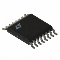
LT3430IFE Linear Technology, LT3430IFE Datasheet - Page 20

LT3430IFE
Manufacturer Part Number
LT3430IFE
Description
IC REG SW STDN 3A 200KHZ 16TSSOP
Manufacturer
Linear Technology
Type
Step-Down (Buck)r
Datasheet
1.LT3430EFE-1PBF.pdf
(28 pages)
Specifications of LT3430IFE
Internal Switch(s)
Yes
Synchronous Rectifier
No
Number Of Outputs
1
Voltage - Output
1.2 ~ 54 V
Current - Output
3A
Frequency - Switching
200kHz
Voltage - Input
5.5 ~ 60 V
Operating Temperature
-40°C ~ 125°C
Mounting Type
Surface Mount
Package / Case
16-TSSOP Exposed Pad, 16-eTSSOP, 16-HTSSOP
Lead Free Status / RoHS Status
Contains lead / RoHS non-compliant
Power - Output
-
Available stocks
Company
Part Number
Manufacturer
Quantity
Price
Part Number:
LT3430IFE
Manufacturer:
LT/凌特
Quantity:
20 000
Company:
Part Number:
LT3430IFE#PBF
Manufacturer:
LT
Quantity:
1 030
Part Number:
LT3430IFE#TRPB
Manufacturer:
LT
Quantity:
20 000
Part Number:
LT3430IFE-1
Manufacturer:
LINEAR/凌特
Quantity:
20 000
Company:
Part Number:
LT3430IFE-1#PBF
Manufacturer:
LT
Quantity:
973
Company:
Part Number:
LT3430IFETR
Manufacturer:
TOSH
Quantity:
4 574
Company:
Part Number:
LT3430IFETRPBF
Manufacturer:
LT
Quantity:
5 574
LT3430/LT3430-1
APPLICATIONS INFORMATION
lower V
losses. In general, the maximum and minimum V
should be checked with maximum typical load current for
calculation of the LT3430/LT3430-1 die temperature. If a
more accurate die temperature is required, a measure-
ment of the SYNC pin resistance (to GND) can be used.
The SYNC pin resistance can be measured by forcing a
voltage no greater than 0.5V at the pin and monitoring the
pin current over temperature in an oven. This should be
done with minimal device power (low V
(V
ambient (oven) temperature.
Note: Some of the internal power dissipation in the IC,
due to BOOST pin voltage, can be transferred outside
of the IC to reduce junction temperature, by increasing
the voltage drop in the path of the boost diode D2 (see
Figure 9). This reduction of junction temperature inside
the IC will allow higher ambient temperature operation for
a given set of conditions. BOOST pin circuitry dissipates
power given by:
Typically V
equals V
considered almost equal, where:
Hence the equation used for boost circuitry power dissi-
pation given in the previous Thermal Calculations section
is stated as:
Here it can be seen that boost power dissipation increases
as the square of V
V
voltage drop in the path of D2. Care should be taken that
V
required for full saturation of the internal power switch.
For output voltages of 5V, V
switch turn on, V
dicharged by the BOOST pin. In the previous BOOST Pin
20
C2
C2
C
V
P
P
below V
= 0V)) in order to calibrate SYNC pin resistance with
DISS
DISS BOOST
C2
does not fall below the minimum 3.3V boost voltage
= V
IN
(
OUT
BOOST Pin =
may generate greater losses due to switch DC
OUT
C2
OUT
. This is because diodes D1 and D2 can be
(the boost voltage across the capacitor C2)
– V
)
to save power dissipation by increasing the
=
C2
FD2
OUT
V
OUT
will fall as the boost capacitor C2 is
– (–V
. It is possible, however, to reduce
V
•
OUT
V
(
I
IN
C2
FD1
SW
is approximately 5V. During
•
) = V
(
/
I
SW
36
V
IN
)
OUT
/
•
36
V
IN
OUT
)
and no switching
•
V
C
2
IN
levels
section, the value of C2 was designed for a 0.7V droop in
V
still allow the minimum 3.3V for the boost function using
the C2 capacitor calculated. If a target output voltage of
12V is required, however, an excess of 8V is placed across
the boost capacitor which is not required for the boost
function but still dissipates additional power.
What is required is a voltage drop in the path of D2 to
achieve minimal power dissipation while still maintaining
minimum boost voltage across C2. A zener, D4, placed in
series with D2 (see Figure 9), drops voltage to C2.
Example : the BOOST pin power dissipation for a 20V input
to 12V output conversion at 2A is given by:
If a 7V zener D4 is placed in series with D2, then power
dissipation becomes :
For an FE package with thermal resistance of 45°C/W,
ambient temperature savings would be, T(ambient) sav-
C2
V
IN
P
P
= V
BOOST
BOOST
DROOP
C3
=
=
Figure 9. BOOST Pin, Diode Selection
. Hence, an output voltage as low as 4V would
12 2 36 12
12 2 36 5
V
SHDN
SYNC
GND
IN
•
•
(
(
LT3430-1
C
LT3430/
BOOST
C
R
20
C
20
/
/
BIAS
V
)
)
SW
C
FB
•
•
C
F
=
=
0 167
0 4
.
.
D1
C2
W
W
D2
D2
L1
R1
R2
3430 F09
D4
+
34301fa
C1
V
OUT


