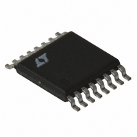
LT3430IFE Linear Technology, LT3430IFE Datasheet - Page 17

LT3430IFE
Manufacturer Part Number
LT3430IFE
Description
IC REG SW STDN 3A 200KHZ 16TSSOP
Manufacturer
Linear Technology
Type
Step-Down (Buck)r
Datasheet
1.LT3430EFE-1PBF.pdf
(28 pages)
Specifications of LT3430IFE
Internal Switch(s)
Yes
Synchronous Rectifier
No
Number Of Outputs
1
Voltage - Output
1.2 ~ 54 V
Current - Output
3A
Frequency - Switching
200kHz
Voltage - Input
5.5 ~ 60 V
Operating Temperature
-40°C ~ 125°C
Mounting Type
Surface Mount
Package / Case
16-TSSOP Exposed Pad, 16-eTSSOP, 16-HTSSOP
Lead Free Status / RoHS Status
Contains lead / RoHS non-compliant
Power - Output
-
Available stocks
Company
Part Number
Manufacturer
Quantity
Price
Part Number:
LT3430IFE
Manufacturer:
LT/凌特
Quantity:
20 000
Company:
Part Number:
LT3430IFE#PBF
Manufacturer:
LT
Quantity:
1 030
Part Number:
LT3430IFE#TRPB
Manufacturer:
LT
Quantity:
20 000
Part Number:
LT3430IFE-1
Manufacturer:
LINEAR/凌特
Quantity:
20 000
Company:
Part Number:
LT3430IFE-1#PBF
Manufacturer:
LT
Quantity:
973
Company:
Part Number:
LT3430IFETR
Manufacturer:
TOSH
Quantity:
4 574
Company:
Part Number:
LT3430IFETRPBF
Manufacturer:
LT
Quantity:
5 574
LAYOUT CONSIDERATIONS
As with all high frequency switchers, when considering
layout, care must be taken in order to achieve optimal
electrical, thermal and noise performance. For maximum
effi ciency, switch rise and fall times are typically in the
nanosecond range. To prevent noise both radiated and
conducted, the high speed switching current path, shown
in Figure 5, must be kept as short as possible. This is
implemented in the suggested layout of Figure 6. Shorten-
APPLICATIONS INFORMATION
AVAILABLE SPACE UNDERNEATH
THE DEVICE BETWEEN PINS AND
SHORTED TOGETHER (USING
SW PINS 2 AND 5 ARE ALSO
ARE SHORTED TOGETHER.
V
IN
GND PLANE)
1
2
3
4
5
6 BOOST
PINS 3 AND 4
GND
SW
V
V
SW
IN
IN
LT3430/
LT3430-1
LT3430/LT3430-1
C3-D1 LOOP
MINIMIZE
GND
V
IN
V
IN
GROUND PINS (4 CORNERS) FOR
GOOD THERMAL CONDUCTIVITY
PLACE FEEDTHROUGH AROUND
D1
C3
Figure 5. High Speed Switching Path
C3
Figure 6. Suggested Layout
CIRCULATING
FREQUENCY
LT3430-1
LT3430/
HIGH
PATH
L1
1
2
3
4
5
6
7
8
GND
SW
V
V
SW
BOOST
GND
C2
IN
IN
LT3430-1
LT3430/
D2
ing this path will also reduce the parasitic trace inductance
of approximately 25nH/inch. At switch off, this parasitic
inductance produces a fl yback spike across the LT3430/
LT3430-1 switch. When operating at higher currents and
input voltages, with poor layout, this spike can generate
voltages across the LT3430/LT3430-1 that may exceed its
absolute maximum rating. A ground plane should always
be used under the switcher circuitry to prevent interplane
coupling and overall noise.
BIAS
GND
GND
FB
V
D1
C
16
15
14
13
12
11
10
L1
9
C1
SHDN
SYNC
R1
C
LOAD
FB
C1
GROUND PLANE
R
C
3430 F05
CONNECT TO
C
C
R2
C
5V
F
LT3430/LT3430-1
KEEP FB AND V
AWAY FROM HIGH FREQUENCY,
HIGH CURRENT COMPONENTS
V
GND
KELVIN SENSE
OUT
V
OUT
3430 F06
SOLDER THE EXPOSED PAD
(PIN 17) TO THE ENTIRE COPPER
GROUND PLANE UNDERNEATH
THE DEVICE. NOTE: THE BOOST
AND BIAS COPPER TRACES ARE
ON A SEPARATE LAYER FROM
THE GROUND PLANE
C
COMPONENTS
17
34301fa


