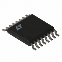
LT3430IFE Linear Technology, LT3430IFE Datasheet - Page 15

LT3430IFE
Manufacturer Part Number
LT3430IFE
Description
IC REG SW STDN 3A 200KHZ 16TSSOP
Manufacturer
Linear Technology
Type
Step-Down (Buck)r
Datasheet
1.LT3430EFE-1PBF.pdf
(28 pages)
Specifications of LT3430IFE
Internal Switch(s)
Yes
Synchronous Rectifier
No
Number Of Outputs
1
Voltage - Output
1.2 ~ 54 V
Current - Output
3A
Frequency - Switching
200kHz
Voltage - Input
5.5 ~ 60 V
Operating Temperature
-40°C ~ 125°C
Mounting Type
Surface Mount
Package / Case
16-TSSOP Exposed Pad, 16-eTSSOP, 16-HTSSOP
Lead Free Status / RoHS Status
Contains lead / RoHS non-compliant
Power - Output
-
Available stocks
Company
Part Number
Manufacturer
Quantity
Price
Part Number:
LT3430IFE
Manufacturer:
LT/凌特
Quantity:
20 000
Company:
Part Number:
LT3430IFE#PBF
Manufacturer:
LT
Quantity:
1 030
Part Number:
LT3430IFE#TRPB
Manufacturer:
LT
Quantity:
20 000
Part Number:
LT3430IFE-1
Manufacturer:
LINEAR/凌特
Quantity:
20 000
Company:
Part Number:
LT3430IFE-1#PBF
Manufacturer:
LT
Quantity:
973
Company:
Part Number:
LT3430IFETR
Manufacturer:
TOSH
Quantity:
4 574
Company:
Part Number:
LT3430IFETRPBF
Manufacturer:
LT
Quantity:
5 574
poor RFI behavior and if the overshoot is severe enough,
damage the IC itself.
The suggested catch diode (D1) is an International Recti-
fi er 30BQ060 Schottky. It is rated at 3A average forward
current and 60V reverse voltage. Typical forward voltage
is 0.52V at 3A. The diode conducts current only during
switch off time. Peak reverse voltage is equal to regulator
input voltage. Average forward current in normal operation
can be calculated from:
This formula will not yield values higher than 3A with
maximum load current of 3A.
BOOST PIN
For most LT 3430 applications, the boost components are
a 0.68µF capacitor and a MMSD914TI diode. The anode
is typically connected to the regulated output voltage to
generate a voltage approximately V
the output stage. However, the output stage discharges
the boost capacitor during the on time of the switch. The
output driver requires at least 3V of headroom throughout
this period to keep the switch fully saturated. If the output
voltage is less than 3.3V, it is recommended that an alternate
boost supply is used. For output voltages greater than 6V,
it is recommended to place a zener diode (D4; page 20)
in series with the Boost diode to set Boost-to-SW voltage
between 4V to 6V. This minimizes power loss within the
IC, improving maximum ambient temperature operation.
In addition, D4 minimizes Boost current overshoot during
power switch turn on to reduce noise within the regula-
tor loop. For output voltages greater than the standard
demoboard 5V output, a location for D4 is provided.
A 0.68µF boost capacitor is recommended for most LT3430
applications. Almost any type of fi lm or ceramic capaci-
tor is suitable, but the ESR should be <1Ω to ensure it
can be fully recharged during the off time of the switch.
The LT3430 capacitor value is derived from conditions of
4800ns on time, 75mA boost current and 0.7V discharge
ripple. The boost capacitor value could be reduced under
APPLICATIONS INFORMATION
I
D AVG
(
)
=
I
OUT
(
V
IN
V
IN
–
V
OUT
)
OUT
above V
IN
to drive
less demanding conditions, but this will not improve cir-
cuit operation or effi ciency. Under low input voltage and
low load conditions, a higher value capacitor will reduce
discharge ripple and improve start-up operation. For the
LT3430-1 a 1.5µF boost capacitor is recommended.
SHUTDOWN FUNCTION AND UNDERVOLTAGE
LOCKOUT
Figure 4 shows how to add undervoltage lockout (UVLO)
to the LT3430/LT3430-1. Typically, UVLO is used in situ-
ations where the input supply is current limited, or has
a relatively high source resistance. A switching regulator
draws constant power from the source, so source cur-
rent increases as source voltage drops. This looks like a
negative resistance load to the source and can cause the
source to current limit or latch low under low source voltage
conditions. UVLO prevents the regulator from operating at
source voltages where these problems might occur.
Threshold voltage for lockout is about 2.38V. A 5.5µA
bias current fl ows out of the pin at this threshold. The
internally generated current is used to force a default high
state on the shutdown pin if the pin is left open. When
low shutdown current is not an issue, the error due to this
current can be minimized by making R
shutdown current is an issue, R
but the error due to initial bias current and changes with
temperature should be considered.
Keep the connections from the resistors to the shutdown
pin short and make sure that interplane or surface capaci-
tance to the switching nodes are minimized. If high resistor
values are used, the shutdown pin should be bypassed with
a 1000pF capacitor to prevent coupling problems from the
switch node. If hysteresis is desired in the undervoltage
lockout point, a resistor R
node. Resistor values can be calculated from:
V
R
R
IN
LO
HI
= Minimum input voltage
=
=
2 38
10
.
R
k
LO
to 100k 25k suggested
V R
(
V
−
IN
−
LO
2 38
(
(
.
5 5
LT3430/LT3430-1
. µ
V
FB
)
A
can be added to the output
)
LO
can be raised to 100k,
)
LO
10k or less. If
15
34301fa


