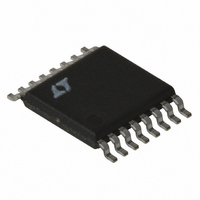
LT3430IFE Linear Technology, LT3430IFE Datasheet - Page 19

LT3430IFE
Manufacturer Part Number
LT3430IFE
Description
IC REG SW STDN 3A 200KHZ 16TSSOP
Manufacturer
Linear Technology
Type
Step-Down (Buck)r
Datasheet
1.LT3430EFE-1PBF.pdf
(28 pages)
Specifications of LT3430IFE
Internal Switch(s)
Yes
Synchronous Rectifier
No
Number Of Outputs
1
Voltage - Output
1.2 ~ 54 V
Current - Output
3A
Frequency - Switching
200kHz
Voltage - Input
5.5 ~ 60 V
Operating Temperature
-40°C ~ 125°C
Mounting Type
Surface Mount
Package / Case
16-TSSOP Exposed Pad, 16-eTSSOP, 16-HTSSOP
Lead Free Status / RoHS Status
Contains lead / RoHS non-compliant
Power - Output
-
Available stocks
Company
Part Number
Manufacturer
Quantity
Price
Part Number:
LT3430IFE
Manufacturer:
LT/凌特
Quantity:
20 000
Company:
Part Number:
LT3430IFE#PBF
Manufacturer:
LT
Quantity:
1 030
Part Number:
LT3430IFE#TRPB
Manufacturer:
LT
Quantity:
20 000
Part Number:
LT3430IFE-1
Manufacturer:
LINEAR/凌特
Quantity:
20 000
Company:
Part Number:
LT3430IFE-1#PBF
Manufacturer:
LT
Quantity:
973
Company:
Part Number:
LT3430IFETR
Manufacturer:
TOSH
Quantity:
4 574
Company:
Part Number:
LT3430IFETRPBF
Manufacturer:
LT
Quantity:
5 574
THERMAL CALCULATIONS
Power dissipation in the LT3430/LT3430-1 chip comes
from four sources: switch DC loss, switch AC loss, boost
circuit current, and input quiescent current. The follow-
ing formulas show how to calculate each of these losses.
These formulas assume continuous mode operation, so
they should not be used for calculating effi ciency at light
load currents.
Switch loss:
(Note: Switching losses are less for the LT3430-1 oper-
ating at only 100kHz)
Boost current loss:
Quiescent current loss:
Example: with V
Total power dissipation in the IC is given by:
APPLICATIONS INFORMATION
P
P
P
SW
Q
BOOST
R
t
t
t
t
f = Switch frequency
P
P
P
P
EFF
r
f
Ir
=
SW
Q
= (t
TOT
BOOST
SW
= (V
= (V
=
=
= t
40 0 0015
=
= Effective switch current/voltage overlap time
0 08 0 72 0 8
(
r
= Switch resistance (≈ 0.15) hot
If
=
( .
=
0 15 2
= P
= 0.8W + 0.04W + 0.08W = 0.92W
V
.
+ t
IN
IN
.
IN
= (I
( ) (
R
/1.1)ns
/1.2)ns
5
=
f
SW
(
SW OUT
+
0 0015
)( ) ( )
40
+ t
2
OUT
V
.
40
OUT
+ P
(
2 36
.
Ir
I
)
IN
2
/0.2)ns
/
+
+ t
5
V
BOOST
2
= 40V, V
5 0 003
=
IN
)
(
V
If
( .
)
) (
I
)
+
+
2
IN
OUT
=
.
(
V
V
90 10
0 04
W
OUT
OUT
+ P
.
/
36
•
)
OUT
=
Q
W
(
)
)
0 003
0 08
−
+
.
9
.
= 5V and I
)
t
( ) ( )( )
EFF
1 2 2 40 200 10
W
/
)
( / )
1 2
(
I
OUT
OUT
(
= 2A:
)( )( )
V
IN
•
f
3
)
Thermal resistance for the LT3430/LT3430-1 package is in-
fl uenced by the presence of internal or backside planes.
TSSOP (Exposed Pad) Package: With a full plane under
the TSSOP package, thermal resistance will be about
45°C/W.
To calculate die temperature, use the proper thermal
resistance number for the desired package and add in
worst-case ambient temperature:
When estimating ambient, remember the nearby catch
diode and inductor will also be dissipating power:
Only a portion of the temperature rise in the external
inductor and diode is coupled to the junction of the
LT3430. Based on empirical measurements, the thermal
effect on the LT3430 junction temperature due to power
dissipation in the external inductor and catch diode can
be calculated as:
Using the example calculations for LT3430 dissipation, the
LT3430 die temperature will be estimated as:
With the TSSOP package (θ
temperature of 50°C:
Die temperature can peak for certain combinations of V
V
switch AC losses, quiescent and catch diode losses, a
OUT
T
V
P
R
P
∆T
T
T
P
P
J
J
J
DIODE
F
DIODE
INDUCTOR
INDUCTOR
IND
J
= T
= T
= 50 + (45 • 0.92) + (5 • 1.31) = 98°C
= Forward voltage of diode (assume 0.52V at 2A)
and load current. While higher V
(LT3430) ≈ (P
= Inductor DC resistance (assume 0.1Ω)
A
A
+ (θ
+ (θ
=
=
( )(
( . )(
V V
0 52 40 5 2
= (I
(2)
JA
JA
F
2
• P
• P
LOAD
(0.1) = 0.4W
IN
40
TOT
TOT
DIODE
–
)
– )( )
V
2
V
)
) + [5 • (P
LT3430/LT3430-1
(R
IN
OUT
IND
+ P
JA
)(
)
I
INDUCTOR
=
LOAD
= 45°C/W), at an ambient
0 91
DIODE
.
)
W
)(5°C/W)
+ P
IN
INDUCTOR
gives greater
19
)]
34301fa
IN
,


