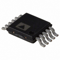
ADP1621ARMZ-R7 Analog Devices Inc, ADP1621ARMZ-R7 Datasheet - Page 4

ADP1621ARMZ-R7
Manufacturer Part Number
ADP1621ARMZ-R7
Description
IC CTRLR DC/DC PWM STEPUP 10MSOP
Manufacturer
Analog Devices Inc
Type
Step-Up (Boost)r
Datasheet
1.ADP1621ARMZ-R7.pdf
(32 pages)
Specifications of ADP1621ARMZ-R7
Internal Switch(s)
No
Synchronous Rectifier
Yes
Number Of Outputs
1
Current - Output
1A
Frequency - Switching
100kHz ~ 1.5MHz
Voltage - Input
2.9 ~ 5.5 V
Operating Temperature
-40°C ~ 125°C
Mounting Type
Surface Mount
Package / Case
10-MSOP, Micro10™, 10-uMAX, 10-uSOP
Primary Input Voltage
5.5V
No. Of Outputs
1
Output Current
1A
No. Of Pins
10
Operating Temperature Range
-40°C To +125°C
Msl
MSL 1 - Unlimited
Frequency Max
1.5MHz
Termination Type
SMD
Lead Free Status / RoHS Status
Lead free / RoHS Compliant
For Use With
ADP1621-EVALZ - BOARD EVALUATION FOR ADP1621
Voltage - Output
-
Power - Output
-
Lead Free Status / RoHS Status
Lead free / RoHS Compliant, Lead free / RoHS Compliant
Other names
ADP1621ARMZ-R7
ADP1621ARMZ-R7TR
ADP1621ARMZ-R7TR
ADP1621
Parameter
GATE DRIVER
1
2
3
4
5
6
7
8
9
The maximum input voltage is the shunt regulation voltage, which is typically 5.5 V and can range from 5.3 V to 6.0 V over the specified temperature range.
The ADP1621 is tested in a feedback servo loop, which servos V
2.9 V to 5 V. The line regulation is calculated by (∆V
The ADP1621 is tested in a feedback servo loop, which servos V
(1.0 V ≤ V
The peak slope-compensation current at the CS pin is typically 70 μA, and effectively clamped at 116 mV. Thus, R
Guaranteed by design for thermal shutdown. When the thermal junction temperature of the ADP1621 reaches approximately 150°C, the ADP1621 goes into thermal
shutdown and the GATE voltage is pulled low. When the junction temperature drops below about 140°C, the soft start sequence is initiated and the ADP1621 resumes
normal operation.
f
Guaranteed by design and bench characterization.
To ensure proper synchronization operation, set the synchronization frequency, f
be synchronized to as high as 1.8 MHz, the peak slope-compensation current decreases at higher synchronization frequencies. It is recommended that the maximum
f
Compensation section in the Application Information: Boost Converter section).
GATE rise and fall times are measured from 10% to 90% levels.
OSC
SYNC
GATE Rise Time
GATE Fall Time
is the natural oscillation frequency, f
be less than 1.4× of f
COMP
≤ 2.0 V).
9
9
OSC
and should not exceed 1.8 MHz. The slope-compensation resistor, R
SYNC
is the synchronization frequency, and f
FB
/V
Symbol
t
t
FB
R
F
) × 100%/∆V
FB
FB
to the internal reference voltage. The voltage change in FB is measured while V
to the internal reference voltage, and V
IN
.
Conditions
C
C
Rev. A | Page 4 of 32
GATE
GATE
SW
= 3.3 nF
= 3.3 nF
is the switching frequency. If synchronization is used, then f
SYNC
, to 1.2× of the free-running frequency, f
S
, should be chosen for the synchronization frequency (see the Slope
COMP
is forced from 1.4 V to 1.5 V. The V
S
should not exceed 1.6 kΩ (116 mV/70 μA).
OSC
Min
. Although the switching frequency can
Typ
17
13
SW
= f
SYNC
COMP
IN
; otherwise, f
is changed from
range is
Max
SW
Unit
ns
ns
= f
OSC
.


