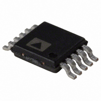
ADP1621ARMZ-R7 Analog Devices Inc, ADP1621ARMZ-R7 Datasheet - Page 23

ADP1621ARMZ-R7
Manufacturer Part Number
ADP1621ARMZ-R7
Description
IC CTRLR DC/DC PWM STEPUP 10MSOP
Manufacturer
Analog Devices Inc
Type
Step-Up (Boost)r
Datasheet
1.ADP1621ARMZ-R7.pdf
(32 pages)
Specifications of ADP1621ARMZ-R7
Internal Switch(s)
No
Synchronous Rectifier
Yes
Number Of Outputs
1
Current - Output
1A
Frequency - Switching
100kHz ~ 1.5MHz
Voltage - Input
2.9 ~ 5.5 V
Operating Temperature
-40°C ~ 125°C
Mounting Type
Surface Mount
Package / Case
10-MSOP, Micro10™, 10-uMAX, 10-uSOP
Primary Input Voltage
5.5V
No. Of Outputs
1
Output Current
1A
No. Of Pins
10
Operating Temperature Range
-40°C To +125°C
Msl
MSL 1 - Unlimited
Frequency Max
1.5MHz
Termination Type
SMD
Lead Free Status / RoHS Status
Lead free / RoHS Compliant
For Use With
ADP1621-EVALZ - BOARD EVALUATION FOR ADP1621
Voltage - Output
-
Power - Output
-
Lead Free Status / RoHS Status
Lead free / RoHS Compliant, Lead free / RoHS Compliant
Other names
ADP1621ARMZ-R7
ADP1621ARMZ-R7TR
ADP1621ARMZ-R7TR
BOOTSTRAPPED BOOST CONVERTER
The inputs of the ADP1621 can be driven from the step-up
converter output voltage to improve efficiency for low input
voltages. For low input voltages, bootstrapped operation improves
efficiency with heavy loads by increasing the available gate drive
voltage, thus reducing the on resistance of the MOSFET. However,
because the internal circuitry is driven from IN, the ADP1621
quiescent current and gate drive current supplied from the input
increases due to the step-up ratio and the conversion efficiency loss.
The circuit shown in Figure 1 shows a bootstrapped boost con-
verter, where V
starts, make sure that the input voltage minus the forward-voltage
drop of the diode is greater than the UVLO voltage and the gate
threshold voltage of the MOFSET. In this example, the MOSFET
has a gate threshold voltage of 2.5 V. The regulator shown in
Figure 1 is very similar to that shown in Figure 33, which is a
standard boost without bootstrapping. Because the same MOSFET
and inductor are used in both circuits and the input and output
conditions are the same, the compensation components remain
unchanged.
Figure 34 shows a bootstrapped application circuit for output
voltages greater than 5.5 V. In this case, the output is 12 V.
Notice that a resistor, R3, of 700 Ω is placed between V
the IN and PIN pins to limit the input currents because the IN
and PIN pins are regulated to 5.5 V. A diode, D2, is placed between
V
to start the ADP1621. Once the ADP1621 starts and the output
IN
and the IN/PIN pins to supply the necessary quiescent current
IN
= 3.3 V and V
OUT
= 5 V. To ensure that the circuit
OUT
and
Rev. A | Page 23 of 32
voltage reaches 12 V, the quiescent current stops flowing
through D2 and is supplied by the output. Keep in mind that the
dynamic supply current to PIN increases as the switching fre-
quency increases because more gate drive is needed for a higher
switching frequency. Therefore, R3 needs to be set appropriately.
The PIN supply current can be approximated by
where I
and Q
An alternative implementation to Figure 34 is shown in Figure 35,
where an NPN transistor is used to supply the necessary current
to the input PIN at various loads, but the gate drive voltage is
limited to approximately 4.8 V (one diode drop below the
voltage at IN). Signal Diodes D2 and D3 help to provide the
necessary quiescent current to start the ADP1621. Once the
ADP1621 starts, the current stops flowing through these two
diodes because the voltages at PIN and IN are approximately
4.8 V and 5.5 V, respectively. One advantage of this technique
is that Q1 provides enough current to the gate driver at any
switching frequency with a wide range of MOSFETs that have
different gate charge specifications.
Notice that the output capacitor, C
is a large aluminum electrolytic capacitor, both in physical size
and capacitance. Such capacitors are very cheap relative to
ceramic capacitors (such as Sanyo POSCAP) or aluminum
polymer capacitors. The ADP1621 can work with a wide range
of capacitor types.
I
G
PIN
PIN
is the gate charge of a particular MOSFET.
is the PIN supply current, f
=
f
SW
×
Q
G
OUT2
SW
in Figure 34 and Figure 35,
is the switching frequency,
ADP1621
(45)


