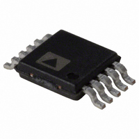
ADP1621ARMZ-R7 Analog Devices Inc, ADP1621ARMZ-R7 Datasheet - Page 21

ADP1621ARMZ-R7
Manufacturer Part Number
ADP1621ARMZ-R7
Description
IC CTRLR DC/DC PWM STEPUP 10MSOP
Manufacturer
Analog Devices Inc
Type
Step-Up (Boost)r
Datasheet
1.ADP1621ARMZ-R7.pdf
(32 pages)
Specifications of ADP1621ARMZ-R7
Internal Switch(s)
No
Synchronous Rectifier
Yes
Number Of Outputs
1
Current - Output
1A
Frequency - Switching
100kHz ~ 1.5MHz
Voltage - Input
2.9 ~ 5.5 V
Operating Temperature
-40°C ~ 125°C
Mounting Type
Surface Mount
Package / Case
10-MSOP, Micro10™, 10-uMAX, 10-uSOP
Primary Input Voltage
5.5V
No. Of Outputs
1
Output Current
1A
No. Of Pins
10
Operating Temperature Range
-40°C To +125°C
Msl
MSL 1 - Unlimited
Frequency Max
1.5MHz
Termination Type
SMD
Lead Free Status / RoHS Status
Lead free / RoHS Compliant
For Use With
ADP1621-EVALZ - BOARD EVALUATION FOR ADP1621
Voltage - Output
-
Power - Output
-
Lead Free Status / RoHS Status
Lead free / RoHS Compliant, Lead free / RoHS Compliant
Other names
ADP1621ARMZ-R7
ADP1621ARMZ-R7TR
ADP1621ARMZ-R7TR
EFFICIENCY CONSIDERATIONS
The efficiency, η, of a dc/dc converter is given by
where P
converter. While switching regulators are ideally lossless converters
of power, the nonideal characteristics of regulator components
degrade the efficiency of the regulator.
The primary sources of power dissipation in the regulator include
•
•
•
The power dissipation in the external power MOSFET due
to conduction and switching losses.
The power dissipation in the external current-sense
resistor if lossless current sensing is not used.
The power dissipation in the external diode.
η
P
MOSFET
=
OUT
P
P
P
P
OUT
IN
CS
DIODE
is the output power, and P
=
=
=
×
⎡
⎢
⎢
⎢
⎢
⎣
P
⎛
⎜
⎝
⎡
⎢
⎣
100
(
⎛
⎜
⎝
C
=
I
1
V
I
LOAD
1
+
−
V
OUT
LOAD
%
−
P
D
D
D
SW
×
+
⎞
⎟
⎠
I
2
⎞
× ⎟
⎠
V
LOAD
×
D
D
D
)
×
×
×
I
R
1
R
LOAD
CS
DSON
−
D
2
×
IN
×
(
1 (
is the input power to the
t
R
+
+
K
t
)
F
⎤
⎥
⎦
)
+
×
f
SW
⎤
⎥
⎥
⎥
⎥
⎦
(38)
(39)
(40)
(41)
Rev. A | Page 21 of 32
•
•
The secondary sources of power dissipation in the regulator include
•
•
The power dissipation in the winding resistance of the
power stage inductor.
The supply current to the ADP1621 IC, which includes the
quiescent current and the gate driver charging current. The
power dissipation due to gate charging loss is approximated by
where P
the PIN pin, Q
the converter switching frequency. Therefore, the total power
dissipation in the IC itself is given by
where P
quiescent current, and V
The power dissipation in the ESR of the input and output
capacitors.
Inductor core losses due to hysteresis and eddy currents.
P
P
P
G
IC
L
,
G
IC
W
=
=
is the gate charging power loss, V
=
is the total power dissipated in the IC, I
V
=
P
(
V
PIN
G
⎛
⎜
⎝
PIN
+
I
1
G
×
LOAD
(
−
V
is the MOSFET total gate charge, and f
×
Q
D
IN
Q
G
G
×
×
⎞
⎟
⎠
2
×
I
f
Q
×
SW
f
)
SW
R
IN
W
is the voltage at the IN pin.
)
+
(
V
IN
×
I
Q
)
PIN
is the voltage at
ADP1621
Q
is the
SW
(42)
(43)
(44)
is


