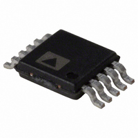
ADP1621ARMZ-R7 Analog Devices Inc, ADP1621ARMZ-R7 Datasheet - Page 27

ADP1621ARMZ-R7
Manufacturer Part Number
ADP1621ARMZ-R7
Description
IC CTRLR DC/DC PWM STEPUP 10MSOP
Manufacturer
Analog Devices Inc
Type
Step-Up (Boost)r
Datasheet
1.ADP1621ARMZ-R7.pdf
(32 pages)
Specifications of ADP1621ARMZ-R7
Internal Switch(s)
No
Synchronous Rectifier
Yes
Number Of Outputs
1
Current - Output
1A
Frequency - Switching
100kHz ~ 1.5MHz
Voltage - Input
2.9 ~ 5.5 V
Operating Temperature
-40°C ~ 125°C
Mounting Type
Surface Mount
Package / Case
10-MSOP, Micro10™, 10-uMAX, 10-uSOP
Primary Input Voltage
5.5V
No. Of Outputs
1
Output Current
1A
No. Of Pins
10
Operating Temperature Range
-40°C To +125°C
Msl
MSL 1 - Unlimited
Frequency Max
1.5MHz
Termination Type
SMD
Lead Free Status / RoHS Status
Lead free / RoHS Compliant
For Use With
ADP1621-EVALZ - BOARD EVALUATION FOR ADP1621
Voltage - Output
-
Power - Output
-
Lead Free Status / RoHS Status
Lead free / RoHS Compliant, Lead free / RoHS Compliant
Other names
ADP1621ARMZ-R7
ADP1621ARMZ-R7TR
ADP1621ARMZ-R7TR
SEPIC CONVERTER CIRCUIT
A single-ended primary inductance converter (SEPIC) topology
is shown in Figure 39. This topology is useful for an unregulated
input voltage, where the regulated output voltage falls within the
input voltage range.
The input and output are dc-isolated by a coupling capacitor,
C5. L1 and L2 are coupled inductors with a 1:1 turn ratio, which
saves space on the PCB. In steady state, the average voltage across
C5 is the input voltage. When the MOSFET turns on and the
diode turns off, the input voltage provides energy to L1, and C5
provides energy to L2. The output capacitor, C
260pF
f
C1 = MURATA GRM32ER60J107ME20
C
C
OSC
OUT2
OUT3
1µF
10V
C3
C2
f
C1 = MURATA GRM332ER61A226K
C
C5 = MURATA GRM21BR61A106K
L1, L2 = COUPLED INDUCTORS, 1:1 RATIO, BH ELECTRONICS BH510-1006
33pF
OSC
= 600kHz
OUT2
1µF
10V
= MURATA GRM21BR60J106K
= SANYO POSCAP 6TPE150MI
C3
C2
= 325kHz
= SANYO POSCAP 6TPE150MI
0.1µF
10V
R
9.4kΩ
C4
C
56nF
COMP
COMP
0.1µF
10V
R
26kΩ
C
1.2nF
C4
COMP
V
COMP
CC
Figure 40. Low Voltage Power-Input Application Circuit
OUT
= 2.9V TO 5.5V
R
31.6kΩ
1%
FREQ
, supplies the
R
65kΩ
SDSN
COMP
FREQ
FREQ
ADP1621
AGND
Figure 39. A SEPIC DC/DC Converter
PIN
SDSN
COMP
FREQ
ADP1621
AGND
GND
PIN
M1 = VISHAY Si7882DP
D1 = MBRD835L
L1 = TOKO FDV0630-2R2M
PGND
GATE
Rev. A | Page 27 of 32
GND
IN
CS
FB
M1 = VISHAY Si7882DP
D1 = VISHAY SSC53L
PGND
GATE
IN
CS
FB
249Ω
R
S
2.4µH
80Ω
R
S
L1
M1
V
L1
2.2µH
IN
load current during this time. When the MOSFET turns off and
the diode turns on, the energy in L1 and L2 is released to charge
the output capacitor, C
well as to supply current to the load.
LOW VOLTAGE POWER-INPUT CIRCUIT
The ADP1621 can be configured to run from a low voltage
(as low as 1 V) power input. The power source generally needs
to have a high current capability, such as a fuel cell. Figure 40
illustrates such an application, where the voltage of the power
input is 1 V and the voltage of the chip supply to the IN and
PIN pins is provided by an auxiliary low power source.
= 1V
V
2.4µH
M1
35.7kΩ
11.5kΩ
D1
IN
L2
= 3V TO 5.5V
C5
10µF
10V
X5R
1%
1%
17.4kΩ
R1
R2
10kΩ
1%
1%
R1
R2
D1
C1
100µF
X5R
6.3V
C
1µF
10V
C
C1
22µF
10V
×2
OUT1
OUT1
1µF
10V
C
10µF
6.3V
V
OUT2
OUT
OUT
2A
V
, and the coupling capacitor, C5, as
= 3.3V
C
150µF
6.3V
×3
OUT
OUT2
1A
C
150µF
6.3V
×2
= 5V
OUT3
ADP1621


