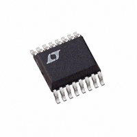
LTC1735IGN#PBF Linear Technology, LTC1735IGN#PBF Datasheet - Page 8

LTC1735IGN#PBF
Manufacturer Part Number
LTC1735IGN#PBF
Description
IC SW REG STEP-DOWN SYNC 16-SSOP
Manufacturer
Linear Technology
Type
Step-Down (Buck)r
Datasheet
1.LTC1735CSPBF.pdf
(32 pages)
Specifications of LTC1735IGN#PBF
Internal Switch(s)
No
Synchronous Rectifier
Yes
Number Of Outputs
1
Voltage - Output
0.8 ~ 6 V
Current - Output
3A
Frequency - Switching
300kHz
Voltage - Input
4 ~ 30 V
Operating Temperature
-40°C ~ 85°C
Mounting Type
Surface Mount
Package / Case
16-SSOP
Number Of Pwm Outputs
1
On/off Pin
No
Adjustable Output
Yes
Topology
Boost/Buck/Flyback
Switching Freq
500KHz
Duty Cycle
99.4%
Operating Supply Voltage (max)
36V
Output Current
3000A
Output Voltage
0.8 to 6V
Synchronous Pin
Yes
Rise Time
50ns
Fall Time
50ns
Operating Temperature Classification
Industrial
Mounting
Surface Mount
Pin Count
16
Package Type
SSOP N
Lead Free Status / RoHS Status
Lead free / RoHS Compliant
Power - Output
-
Lead Free Status / Rohs Status
Compliant
Available stocks
Company
Part Number
Manufacturer
Quantity
Price
PI FU CTIO S
LTC1735
V
resistive divider across the output.
SENSE
SENSE
offsets between SENSE
with R
PGOOD (LTC1735F Only): Open-Drain Logic Output.
PGOOD is pulled to ground when the voltage on the
V
EXTV
This switch closes and supplies V
EXTV
Applications Information section. Do not exceed 7V on
this pin and ensure EXTV
PGND: Driver Power Ground. Connects to the source of
bottom N-channel MOSFET, the anode of the Schottky
diode, and the (–) terminal of C
BG: High Current Gate Drive for Bottom
N-Channel MOSFET. Voltage swing at this pin is from
ground to INTV
8
OSENSE
OSENSE
U
CC
CC
SENSE
–
+
: Input to the Internal Switch Connected to INTV
: The (+) Input to the Current Comparator. Built-in
is higher than 4.7V. See EXTV
: Receives the feedback voltage from an external
: The (–) Input to the Current Comparator.
pin is not within 7.5% of its set point.
U
set the current trip threshold.
CC
.
U
–
and SENSE
CC
V
IN
IN
.
.
+
CC
CC
pins in conjunction
power whenever
connection in the
CC
.
INTV
Switch. The driver and control circuits are powered from
this voltage. Decouple to power ground with a 1 F ceramic
capacitor placed directly adjacent to the IC together with a
minimum of 4.7 F tantalum or other low ESR capacitor.
V
ground.
SW: Switch Node Connection to Inductor and Bootstrap
Capacitor. Voltage swing at this pin is from a Schottky
diode (external) voltage drop below ground to V
BOOST: Supply to Topside Floating Driver. The bootstrap
capacitor is returned to this pin. Voltage swing at this pin
is from a diode drop below INTV
TG: High Current Gate Drive for Top N-Channel MOSFET.
This is the output of a floating driver with a voltage swing
equal to INTV
SW.
IN
: Main Supply Pin. Must be closely decoupled to power
CC
: Output of the Internal 5.2V Regulator and EXTV
CC
superimposed on the switch node voltage
CC
to (V
IN
+ INTV
IN
CC
.
).
1735fc
CC


