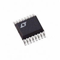
LTC1735IGN#PBF Linear Technology, LTC1735IGN#PBF Datasheet - Page 21

LTC1735IGN#PBF
Manufacturer Part Number
LTC1735IGN#PBF
Description
IC SW REG STEP-DOWN SYNC 16-SSOP
Manufacturer
Linear Technology
Type
Step-Down (Buck)r
Datasheet
1.LTC1735CSPBF.pdf
(32 pages)
Specifications of LTC1735IGN#PBF
Internal Switch(s)
No
Synchronous Rectifier
Yes
Number Of Outputs
1
Voltage - Output
0.8 ~ 6 V
Current - Output
3A
Frequency - Switching
300kHz
Voltage - Input
4 ~ 30 V
Operating Temperature
-40°C ~ 85°C
Mounting Type
Surface Mount
Package / Case
16-SSOP
Number Of Pwm Outputs
1
On/off Pin
No
Adjustable Output
Yes
Topology
Boost/Buck/Flyback
Switching Freq
500KHz
Duty Cycle
99.4%
Operating Supply Voltage (max)
36V
Output Current
3000A
Output Voltage
0.8 to 6V
Synchronous Pin
Yes
Rise Time
50ns
Fall Time
50ns
Operating Temperature Classification
Industrial
Mounting
Surface Mount
Pin Count
16
Package Type
SSOP N
Lead Free Status / RoHS Status
Lead free / RoHS Compliant
Power - Output
-
Lead Free Status / Rohs Status
Compliant
Available stocks
Company
Part Number
Manufacturer
Quantity
Price
APPLICATIO S I FOR ATIO
Although all dissipative elements in the circuit produce
losses, 4 main sources usually account for most of the
losses in LTC1735 circuits: 1) V
current, 3) I
losses.
1) The V
electrical characteristics which excludes MOSFET driver
and control currents. V
loss that increases with V
2) INTV
control currents. The MOSFET driver current results from
switching the gate capacitance of the power MOSFETs.
Each time a MOSFET gate is switched from low to high to
low again, a packet of charge dQ moves from INTV
ground. The resulting dQ/dt is a current out of INTV
is typically much larger than the control circuit current. In
continuous mode, I
are the gate charges of the topside and bottom-side
MOSFETs.
Supplying INTV
from an output-derived or other high efficiency source will
scale the V
circuits by a factor of (Duty Cycle)/(Efficiency). For ex-
ample, in a 20V to 5V application, 10mA of INTV
results in approximately 3mA of V
the mid-current loss from 10% or more (if the driver was
powered directly from V
3) I
MOSFET, inductor and current shunt. In continuous mode
the average output current flows through L and R
but is “chopped” between the topside main MOSFET and
the synchronous MOSFET. If the two MOSFETs have
approximately the same R
one MOSFET can simply be summed with the resistances
of L and R
R
the total resistance is 0.09 . This results in losses ranging
from 2% to 9% as the output current increases from 1A to
5A for a 5V output, or a 3% to 14% loss for a 3.3V output.
Effeciency varies as the inverse square of V
same external components and output power level. I
losses cause the efficiency to drop at high output currents.
DS(ON)
2
R losses are predicted from the DC resistances of the
CC
= 0.03 , R
IN
SENSE
current is the sum of the MOSFET driver and
IN
current is the DC supply current given in the
2
current required for the driver and control
R losses, 4) Topside MOSFET transition
CC
to obtain I
power through the EXTV
GATECHG
U
L
= 0.05 and R
IN
current results in a small (<0.1%)
IN
IN
U
) to only a few percent.
2
DS(ON)
R losses. For example, if each
.
= f(Q
T
, then the resistance of
IN
+Q
IN
W
current. This reduces
SENSE
B
current, 2) INTV
), where Q
CC
= 0.01 , then
switch input
OUT
CC
U
T
current
and Q
for the
CC
SENSE
CC
that
2
CC
to
R
B
,
4) Transition losses apply only to the topside MOSFET(s)
and only become significant when operating at high input
voltages (typically 12V or greater). Transition losses can
be estimated from:
Other “hidden” losses such as copper trace and internal
battery resistances can account for an additional 5% to
10% efficiency degradation in portable systems. It is very
important to include these “system” level losses in the
design of a system. The internal battery and fuse resis-
tance losses can be minimized by making sure that C
adequate charge storage and very low ESR at the switch-
ing frequency. A 25W supply will typically require a
minimum of 20 F to 40 F of capacitance having a maxi-
mum of 0.01 to 0.02 of ESR. Other losses including
Schottky conduction losses during dead-time and induc-
tor core losses generally account for less than 2% total
additional loss.
Checking Transient Response
The regulator loop response can be checked by looking at
the load current transient response. Switching regulators
take several cycles to respond to a step in load current.
When a load step occurs, V
to I
tance of C
C
regulator to adapt to the current change and return V
to its steady-state value. During this recovery time V
can be monitored for excessive overshoot or ringing,
which would indicate a stability problem. OPTI-LOOP
compensation allows the transient response to be opti-
mized over a wide range of output capacitance and ESR
values. The availability of the I
optimization of control loop behavior but also provides a
DC coupled and AC filtered closed loop response test
point. The DC step, rise time and settling at this test point
truly reflects the closed loop response. Assuming a pre-
dominantly second order system, phase margin and/or
damping factor can be estimated using the percentage of
overshoot seen at this pin. The bandwidth can also be
estimated by examining the rise time at the pin. The I
external components shown in the Figure 1 circuit will
provide an adequate starting point for most applications.
OUT
Transition Loss = (1.7) V
LOAD
, generating the feedback error signal that forces the
OUT
(ESR), where ESR is the effective series resis-
. I
LOAD
also begins to charge or discharge
OUT
IN
2
shifts by an amount equal
I
O(MAX)
TH
pin not only allows
C
LTC1735
RSS
f
21
IN
1735fc
has
OUT
OUT
TH


