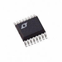
LTC1735IGN#PBF Linear Technology, LTC1735IGN#PBF Datasheet - Page 23

LTC1735IGN#PBF
Manufacturer Part Number
LTC1735IGN#PBF
Description
IC SW REG STEP-DOWN SYNC 16-SSOP
Manufacturer
Linear Technology
Type
Step-Down (Buck)r
Datasheet
1.LTC1735CSPBF.pdf
(32 pages)
Specifications of LTC1735IGN#PBF
Internal Switch(s)
No
Synchronous Rectifier
Yes
Number Of Outputs
1
Voltage - Output
0.8 ~ 6 V
Current - Output
3A
Frequency - Switching
300kHz
Voltage - Input
4 ~ 30 V
Operating Temperature
-40°C ~ 85°C
Mounting Type
Surface Mount
Package / Case
16-SSOP
Number Of Pwm Outputs
1
On/off Pin
No
Adjustable Output
Yes
Topology
Boost/Buck/Flyback
Switching Freq
500KHz
Duty Cycle
99.4%
Operating Supply Voltage (max)
36V
Output Current
3000A
Output Voltage
0.8 to 6V
Synchronous Pin
Yes
Rise Time
50ns
Fall Time
50ns
Operating Temperature Classification
Industrial
Mounting
Surface Mount
Pin Count
16
Package Type
SSOP N
Lead Free Status / RoHS Status
Lead free / RoHS Compliant
Power - Output
-
Lead Free Status / Rohs Status
Compliant
Available stocks
Company
Part Number
Manufacturer
Quantity
Price
APPLICATIO S I FOR ATIO
voltage cannot exceed 0.082V. At V
maximum output voltage change controlled by the I
would be:
With the optimum resistor values at the I
voltage will swing from 1.55V at minimum load to 1.44V
at full load. At this output voltage, active voltage position-
ing provides an additional 56mV to the allowable tran-
sient voltage on the output capacitors, a 68% improve-
ment over the 82mV allowed without active voltage
positioning.
The next step is to calculate the scale factor for V
I
TH
100pF
0.1 F
47pF
C5
C2
C4
pin voltage. The V
V
100k
27k
R1
R2
OSENSE
100pF
39pF
1000pF
C1
C3
C6
Input Offset V
0 03
1
2
3
4
5
6
7
8
U
.
0 8
C
RUN/SS
I
FCB
SGND
V
SENSE
SENSE
TH
.
OSC
OSENSE
ITH
V
V
V
REF
LTC1735
• .
–
+
680k
100k
scale factor reflects the I
U
R3
R4
1 5
U1
Figure 8. CPU-Core-Voltage Regulator with Active Voltage Positioning
•
EXTV
BOOST
INTV
PGND
OUT
SW
V
BG
TG
CC
CC
IN
56
16
15
14
13
12
11
10
9
W
mV
5V (OPTIONAL)
TH
OUT
pin, the output
C9
1 F
D1
CMDSH-3
= 1.5V, the
U
+
C8
0.22 F
C7
0.1 F
ITH
TH
TH
C10
4.7 F
10V
, the
pin
pin
M1
FDS6680A
MBRS340
M2, M3
FDS6680A
2
voltage required for a given load current. V
peak sense resistor voltage, which represents the DC
output current plus one half of the peak-to-peak inductor
current. The no load to full load V
2.4V, which controls the sense resistor voltage from 0V to
the V
scale factor with a 0.003 sense resistor is:
V
V
ITH
ITH
V
D2
ITH
at any load current is:
Scale Factor
SENSE(MAX)
C9, C19: TAIYO YUDEN JMK107BJ105
C10: KEMET T494A475M010AS
C12 TO C14: TAIYO YUDEN GMK325F106
C15 TO C18: PANASONIC EEFUE0G181R
D1: CENTRAL SEMI CMDSH-3
D2: MOTOROLA MBRS340
L1: PANASONIC ETQP6F1R0SA
M1 TO M3: FAIRCHILD FDS6680A
R5: IRC LRF2512-01-R003-J
U1: LINEAR TECHNOLOGY LTC1735CS
1 H
L1
V
I
ITH
OUTDC
Offset
0.003
R5
voltage of 75mV. The calculated V
( .
V
2 4
ITH
2
I
L
V
Range Sense
1735 F08
– .
C11
330pF
11.5k
•
0 075
10k
0 3
.
V
R6
R7
ITH
V
ITH
•
V
+
) • .
V
Scale Factor
SENSE MAX
range is from 0.3V to
0 003
C15 TO
C18
180 F
4V
LTC1735
(
C12 TO C14
10 F
35V
Re
ITH
sistor Value
controls the
)
0 084
C19
1 F
.
23
V
7.5V TO
24V
GND
V
1.5V
15A
GND
V A
IN
OUT
1735fc
/
ITH


