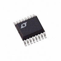
LTC1735IGN#PBF Linear Technology, LTC1735IGN#PBF Datasheet - Page 27

LTC1735IGN#PBF
Manufacturer Part Number
LTC1735IGN#PBF
Description
IC SW REG STEP-DOWN SYNC 16-SSOP
Manufacturer
Linear Technology
Type
Step-Down (Buck)r
Datasheet
1.LTC1735CSPBF.pdf
(32 pages)
Specifications of LTC1735IGN#PBF
Internal Switch(s)
No
Synchronous Rectifier
Yes
Number Of Outputs
1
Voltage - Output
0.8 ~ 6 V
Current - Output
3A
Frequency - Switching
300kHz
Voltage - Input
4 ~ 30 V
Operating Temperature
-40°C ~ 85°C
Mounting Type
Surface Mount
Package / Case
16-SSOP
Number Of Pwm Outputs
1
On/off Pin
No
Adjustable Output
Yes
Topology
Boost/Buck/Flyback
Switching Freq
500KHz
Duty Cycle
99.4%
Operating Supply Voltage (max)
36V
Output Current
3000A
Output Voltage
0.8 to 6V
Synchronous Pin
Yes
Rise Time
50ns
Fall Time
50ns
Operating Temperature Classification
Industrial
Mounting
Surface Mount
Pin Count
16
Package Type
SSOP N
Lead Free Status / RoHS Status
Lead free / RoHS Compliant
Power - Output
-
Lead Free Status / Rohs Status
Compliant
Available stocks
Company
Part Number
Manufacturer
Quantity
Price
APPLICATIO S I FOR ATIO
the INTV
performance.
6) Keep the switching node (SW), top gate node (TG) and
boost node (BOOST) away from sensitive small-signal
nodes, especially from the voltage and current sensing
CC
and PGND pins can help improve noise
U
C
C
R
SS
C2
C
1000pF
U
47pF
C
C
C
OSC
1
2
3
4
5
6
7
8
W
C
RUN/SS
I
FCB
SGND
V
SENSE
SENSE
TH
OSC
OSENSE
LTC1735
–
+
Figure 12. LTC1735 Layout Diagram
Figure 13. Kelvin Sensing R
EXTV
INTV
BOOST
PGND
U
SW
V
BG
TG
CC
CC
IN
16
15
14
13
12
11
10
9
HIGH CURRENT PATH
R1
R2
SENSE
+
+
+
SENSE
C
4.7 F
feedback pins. All of these nodes have very large and fast
moving signals and therefore should be kept on the
“output side” (Pin 9 to Pin 16) of the LTC1735 and occupy
minimum PC trace area.
OUT
D
B
–
M1
C
SENSE
B
CURRENT SENSE
RESISTOR
(R
SENSE
R
L1
SENSE
1735 F13
)
D1
M2
C
IN
1735 F12
V
V
OUT
+
–
–
+
IN
LTC1735
27
1735fc


