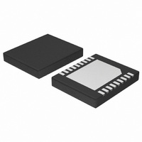
NCP5220MNR2G ON Semiconductor, NCP5220MNR2G Datasheet - Page 5

NCP5220MNR2G
Manufacturer Part Number
NCP5220MNR2G
Description
IC CTLR PWM DUAL BUCK PWR 20-DFN
Manufacturer
ON Semiconductor
Datasheet
1.NCP5220MNR2G.pdf
(18 pages)
Specifications of NCP5220MNR2G
Applications
Controller, DDR
Voltage - Input
5 ~ 12 V
Number Of Outputs
2
Operating Temperature
0°C ~ 70°C
Mounting Type
Surface Mount
Package / Case
20-TFDFN
Switching Frequency
250 KHz
Operating Temperature Range
0 C to + 70 C
Mounting Style
SMD/SMT
Duty Cycle (max)
100%
Lead Free Status / RoHS Status
Lead free / RoHS Compliant
Voltage - Output
-
Lead Free Status / Rohs Status
Lead free / RoHS Compliant
Other names
NCP5220MNR2G
NCP5220MNR2GOSTR
NCP5220MNR2GOSTR
Available stocks
Company
Part Number
Manufacturer
Quantity
Price
Company:
Part Number:
NCP5220MNR2G
Manufacturer:
SIPEX
Quantity:
4 100
ELECTRICAL CHARACTERISTICS
COUT2 = 470 mF, COUT3 = NA, CSS = 33 nF, R1 = 2.166 kW, R2 = 2.0 kW, RZ1 = 20 kW, RZ2 = 8.0 W, CP1 = 10 nF,
CZ1 = 6.8 nF, CZ2 = 100 nF, RM1 = 2.166 kW, RM2 = 2.0 kW, RZM1 = 20 kW, RZM2 = 8.0 W, CPM1 = 10 nF, CZM1 = 6.8 nF,
CZM2 = 100 nf for min/max values unless otherwise noted). Duplicate component values of MCH regulator from DDQ.
SUPPLY VOLTAGE
SUPPLY CURRENT
UNDERVOLTAGE−MONITOR
THERMAL SHUTDOWN
DDQ SWITCHING REGULATOR
DDQ ERROR AMPLIFIER
3. Guaranteed by design, not tested in production.
5VDUAL Operating Voltage
BOOT Operating Voltage
S0 Mode Supply Current from 5VDUAL
S3 Mode Supply Current from 5VDUAL
S5 Mode Supply Current from 5VDUAL
S0 Mode Supply Current from BOOT
S3 Mode Supply Current from BOOT
5VDUAL UVLO Upper Threshold
5VDUAL UVLO Hysteresis
BOOT UVLO Upper Threshold
BOOT UVLO Hysteresis
Thermal Shutdown
Thermal Shutdown Hysteresis
FBDDQ Feedback Voltage, Control Loop in
Regulation
Feedback Input Current
Oscillator Frequency in S0 Mode
Oscillator Frequency in S3 Mode
Oscillator Ramp Amplitude
Current Limit Blanking Time in S0 Mode
Current Limit Threshold Offset from 5VDUAL
Minimum Duty Cycle
Maximum Duty Cycle
Soft−Start Pin Current for DDQ
DC Gain
Gain−Bandwidth Product
Slew Rate
Characteristic
(5VDUAL = 5.0 V, BOOT = 12 V, T
VBOOTUV+
V5VDLUV+
VBOOThys
IBOOT_S0
IBOOT_S3
V5VDLhys
V5VDUAL
I5VDL_S0
I5VDL_S3
I5VDL_S5
GAINDDQ
GBWDDQ
FDDQS0
FDDQS3
TDDQbk
IDDQFB
Symbol
VBOOT
SRDDQ
dVOSC
Tsdhys
VOCP
VFBQ
Dmax
Dmin
Iss1
Tsd
http://onsemi.com
NCP5220
5
BOOT = 12 V, TG_1P5 and BG_1P5
BOOT = 12 V, TG_1P5 and BG_1P5
SLP_S5 = HIGH, SLP_S3 = HIGH,
SLP_S5 = HIGH, SLP_S3 = HIGH,
SLP_S5 = HIGH, SLP_S3 = LOW,
SLP_S5 = HIGH, SLP_S3 = LOW,
SLP_S5 = LOW, BOOT = 0 V,
COMP PIN to GND = 220 nF,
COMP PIN TO GND = 10 pF
TG_1P5 and BG_1P5 Open
TG_1P5 and BG_1P5 Open
TG_1P5 and BG_1P5 Open
1.0 W in Series (Note 3)
A
V(FBDDQ) = 1.3 V
Test Conditions
T
= 0°C to 70°C, L = 1.7 mH, COUT1 = 3770 mF,
A
V(SS) = 0.5 V
= 0°C to 70°C
T
(Note 3)
(Note 3)
(Note 3)
(Note 3)
(Note 3)
(Note 3)
A
Open
Open
= 25°C
1.178
1.166
Min
250
217
434
400
4.5
0.8
0
1.190
12.0
Typ
400
145
250
500
5.0
1.0
1.3
4.0
8.0
25
70
12
1.202
1.214
Max
13.2
10.4
550
283
566
100
5.5
5.0
1.0
4.4
1.0
10
25
25
Vp−p
V/uS
Unit
MHz
KHz
KHz
mA
mA
mA
mA
mA
mV
mA
nS
mA
dB
°C
°C
%
%
V
V
V
V
V
V
V


