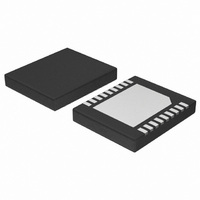
NCP5220MNR2G ON Semiconductor, NCP5220MNR2G Datasheet

NCP5220MNR2G
Specifications of NCP5220MNR2G
NCP5220MNR2GOSTR
Available stocks
Related parts for NCP5220MNR2G
NCP5220MNR2G Summary of contents
Page 1
... NOTE: Pin 21 is the thermal pad on the bottom of the device. ORDERING INFORMATION Device Package NCP5220MNR2 DFN−20 NCP5220MNR2G DFN−20 (Pb−Free) †For information on tape and reel specifications, including part orientation and tape sizes, please refer to our Tape and Reel Packaging Specification Brochure, BRD8011/D. ...
Page 2
SLP_S3 SLP_S3 SLP_S5 SLP_S5 CSS VTT 1.25 V, 2.0 Apk COUT2 CZM2 CZM1 COMP_1P5 R5 CPM1 RZM2 RZM1 5VDUAL R6 TG_1P5 M3 VMCH L 1 BG_1P5 COUT3 M4 NCP5220 BOOT SS 5VDUAL VTT TG_DDQ FBVTT AGND SW_DDQ ...
Page 3
VREF VOLTAGE and CURRENT _VREFGD REFERENCE SLP_S5 SLP_S3 VCC _BOOTGD BOOT_ R10 UVLO VREF R11 5VDUAL R12 5VDUAL_ UVLO VREF R13 _5VDLGD SS OSC S0 CSS S3 1805 Phase Shift S0 VTT Regulation Control AGND NCP5220 THERMAL SHUTDOWN TSD S0 ...
Page 4
PIN DESCRIPTION Pin Symbol 1 COMP VDDQ error amplifier compensation node. 2 FBDDQ DDQ regulator feedback pin Soft−start pin of DDQ and MCH. 4 PGND Power ground. 5 VTT VTT regulator output. 6 VDDQ Power input for VTT ...
Page 5
ELECTRICAL CHARACTERISTICS (5VDUAL = 5.0 V, BOOT = COUT2 = 470 mF, COUT3 = NA, CSS = 33 nF 2.166 kW 2.0 kW, RZ1 = 20 kW, RZ2 = 8.0 W, CP1 = ...
Page 6
ELECTRICAL CHARACTERISTICS (5VDUAL = 5.0 V, BOOT = COUT2 = 470 mF, COUT3 = NA, CSS = 33 nF 2.166 kW 2.0 kW, RZ1 = 20 kW, RZ2 = 8.0 W, CP1 = ...
Page 7
TYPICAL OPERATING CHARACTERISTICS 1.196 1.195 1.194 1.193 1.192 1.191 1.190 1.189 1.188 1.187 AMBIENT TEMPERATURE (°C) A Figure 3. VFBQ Feedback Voltage vs. Ambient Temperature 0.809 0.807 0.805 0.803 0.801 0.799 0.797 0.795 0 20 ...
Page 8
TYPICAL OPERATING WAVEFORMS Channel 1: VDDQ Output Voltage, 1.0 V/div Channel 2: VTT Output Voltage, 1.0 V/div Channel 3: V1P5 Output Voltage, 1.0V/div Time Base: 5.0 ms/div Figure 9. Power−Up Sequence 500 mA Applied to VDDQ 417 mA Applied to ...
Page 9
TYPICAL OPERATING WAVEFORMS Channel 1: Current Sunk into VTT, 2.0 A/div Channel 2: VDDQ output Voltage, AC−Coupled, 100 mV/div Channel 3: VTT Output Voltage, AC−Coupled, 50 mV/div Channel 4: V1P5 Vutput Voltage, AC−Coupled, 100 mV/div Time Base: 200 ms/div Figure ...
Page 10
General The NCP5220 3−in−1 PWM Dual Buck Linear DDR Power Controller contains two high efficiency PWM controllers and an integrated two−quadrant linear regulator. The VDDQ supply is produced by a PWM switching controller with two external N−Ch FETs. The VTT ...
Page 11
For enhanced efficiency, an active synchronous switch is used to eliminate the conduction loss contributed by the forward voltage of a diode or Schottky diode rectifier. Adaptive non−overlap timing control of the complementary gate drive output signals is provided to ...
Page 12
V SLP_S5 SLP_S3 SS Pin DDQ−S0 VTT MCH State 5VSTBY or 5VSTB is the ultimate chip enable, SLP_S5 and SLP_S3 go HIGH. This supply has ...
Page 13
SLP_S3 = 1 AND SLP_S5 = 1 AND _BOOTGD = 1 SLP_S3 = 1 AND SLP_S5 = 1 AND _BOOTGD = 1 NOTE: 5VDUAL is assumed good conditions in any mode. All possible state transitions are shown. ...
Page 14
Application Circuit Figure 20, on the following page, shows the typical application circuit for NCP5220. The NCP5220 is specifically designed as a total power solution for the MCH and DDR memory system. This diagram contains NCP5220 for driving four external ...
Page 15
NCP5220 http://onsemi.com 15 ...
Page 16
... ECJ1VB1A224K 4.7 mF, 6 ECJHVB0J475M 10 mF ECJ4YB1E106M 22 nF ECJ1VB1E223K 6.8 nF ECJ1VB1H682K 100 nF ECJ1VB1C104K 10 nF ECJ1VB1H103K 33 nF ECJ1VB1E333K http://onsemi.com 16 Manufactur ON Semiconductor ON Semiconductor ON Semiconductor ON Semiconductor ON Semiconductor Panasonic Panasonic Panasonic Panasonic Panasonic Panasonic Panasonic Panasonic Panasonic Panasonic Panasonic Panasonic Panasonic Panasonic ...
Page 17
PIN DFN, DUAL−SIDED, 5x6 PIN 1 LOCATION TOP VIEW 0. SIDE VIEW (A3 20X 20X 20 11 ...
Page 18
... Fax: 480−829−7709 or 800−344−3867 Toll Free USA/Canada Email: orderlit@onsemi.com NCP5220 N. American Technical Support: 800−282−9855 Toll Free USA/Canada Japan: ON Semiconductor, Japan Customer Focus Center 2−9−1 Kamimeguro, Meguro−ku, Tokyo, Japan 153−0051 Phone: 81−3−5773−3850 http://onsemi.com 18 ON Semiconductor Website: http://onsemi ...


